What’s MAP-BGA?
The MAP-BGA, or MAPBGA (Mold Array Process Ball Grid Array) package is a surface mount package that uses a grid of solder balls for electrical connections. The individual units are arranged in a matrix array on a substrate strip which are molded together, and then singulated by sawing. Singulated units are distinguished by mold compound completely covering the substrate.
Industry standard MAPBGA sizes and thicknesses are with various options of I/O (solder balls) quantity and pitch. Package sizes range from 3 mm x 3 mm to 27 mm x 27mm with ball pitch ranging from 0.4 mm to 1.27 mm pitch.
The cross-section drawing in Figure below shows the representative internal layers of a typical MAPBGA package with a 2-layer substrate and wirebond interconnects.
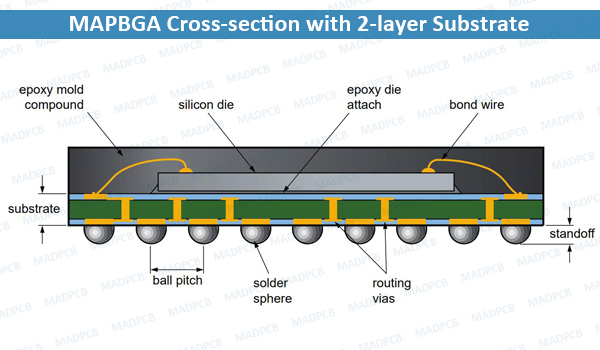
MAPBGA Cross-section with 2-layer Substrate
PCB Design Guidelines
Proper PCB footprint and stencil designs are critical to ensure high SMT assembly yields, and electrical and mechanical performance. The design starts with obtaining the correct package drawing.
PCB Pad Design
MADPCB follows the IPC-7351B, Generic Requirements for Surface Mount Design and Land Pattern Standards. This document and an accompanying land pattern calculator can be purchased from the IPC website and includes guidelines for BGAs based on assumed package dimensions.
Many MAP-BGA products do not have fully populated arrays to allow for better PCB routing. PCB design must ensure the final footprint matches the part.
Pad Diameter
For pitches at or above 0.80mm, the first estimate for PCB solderable diameter is one half the pitch. For pitches at or below 0.65mm, the solderable diameter is generally larger than one-half pitch in diameter.
|
Suggested PCB Pad Diameters by BGA Pitch |
|
| BGA Pitch (mm) |
Suggested PCB Pad Diameter |
|
1.00 |
0.500 |
| 0.80 |
4.000 |
|
0.65 |
0.325 |
| 0.50 |
0.300 |
|
0.40 |
0.225 |
Pad Surface Finishes
Almost all PCB finishes are compatible with MAP-BGAs including Hot Air Solder Leveled (HASL), Organic Solderability Preservative (OSP), Electroless Nickel Immersion Gold (ENIG), Immersion Sn and Immersion Ag. We suggest monitoring the PCB surface finish shelf life to ensure that the life has not “expired”. Surfaces should always be free of dirt and grease before PCB assembly.
Solder Mask Layer
We encourage customers to use Non-Solder Mask Defined (NSMD) PCB pad designs which typically provide better thermal fatigue life. Some field use conditions may require the use of Solder Mask Defined (SMD) pads for better drops/shock survivability. The difference between NSMD and SMD is shown in following figure.
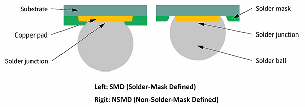
Solder-Mask-Defined (SMD) and Non-Solder-Mask-Defined (NSMD) BGA packages.
The NSMD solder mask opening diameter is suggested to be 0.125mm larger than the solderable area. However, it is critical to understand the PCB manufacturing capabilities of PCB suppliers. Also, finer BGA pitches may require <0.125mm (5mil) in order to meet PCB routing requirements.
SMD pads (compared to NSMD) have a larger Cu diameter which means more Cu is joined to the PCB laminate. Copper diameter for SMD is 0.125mm larger than solder mask opening diameter. This increased diameter makes pad cratering on the PCB more difficult, and therefore increases drop/shock life. For SMD at smaller pitches, a key factor of picking the Cu diameter and solder mask diameter is PCB vendor capabilities. Inspection of delivered PCBs for solder mask registration is encouraged.
Circuit Board Assembly
Stencil Thickness
Solder paste stencil design is critical for good solder joint formation, especially as the BGA pitch decreases. The thickness of the stencil of the stencil determines the amount of solder paste deposited onto the printed circuit board land pattern.
For 1.0mm pitch parts, a common stencil thickness is 0.125mm (5mil), while 0.10mm thick stencils (4mil) are also used. In high reliability applications, 0.15mm (6mil) thick stencils are preferred. For 0.80mm pitch, the 0.1mm thick stencil is common.
For these stencils, well cut openings created with a laser or by chemical etch is preferred. The opening walls should be polished and a nickel (Ni) finish is recommended. The goal is to have a stencil that properly releases a consistent volume of solder paste, print after print.
The stencils for BGA pitches at or below 0.65mm have to consider other factors as well. Usually on a circuit board, there may be other small size and small pitch components that prevent reduction of the stencil opening size. Instead, the total thickness is decreased. Typically, stencils are from 0.075mm (3mil) to 0.125mm (5mil) thick.
At smaller pitches, it may help to use square openings in place of round. Square openings allow a slightly larger volume of solder paste to be released. Generally, the openings allow a slightly larger volume of solder paste to be released. Generally, the opening length or diameter is 1:1 with solderable PCB diameter. For additional solder paste volume, the opening length/diameter could be increased.
Small pitch stencils frequently have specialized coatings to help with paste release. These coatings, frequently called nano-coatings, wear out. A monitoring program for stencil age (number of prints) may be needed.
Solder Paste Properties
Solder paste is one of the most important materials in the SMT assembly process. It is a homogenous mixture of metal alloy, flux, and viscosity modifiers. The metal alloy particles are made in specific size and shape. Flux has a direct effect on soldering and cleaning, and it is used to precondition the surfaces for soldering (by removing minor surface contamination and oxidation).
There are two different flux systems commonly available:
- The 1st requires cleaning such as standard rosin chemistries and water-soluble chemistries. Standard rosin chemistries are normally cleaned with solvents, semi-aqueous solutions, or aqueous/sappnifier solutions, while the water-soluble chemistries are cleaned with pure water.
- The 2nd type of flux system type requires no cleaning, but normally a little residue remains on the PCB after soldering.
Solder paste grain size can be useful to manipulate by pitch. For larger pitch parts, 0.80mm and larger, Type 3 solder powder (25 micron to 45micron grain size) is widely used. At the pitches, 0.65mm and smaller, Type 4 solder (20micron to 38micron grain size) may provide a better solder joint.