What’s Photoconductivity?
Photoconductivity is an optical and electrical phenomenon in which a material becomes more electrically conductive due to the absorption of electromagnetic radiation such as visible light, ultraviolet light, infrared light, or gamma radiation.
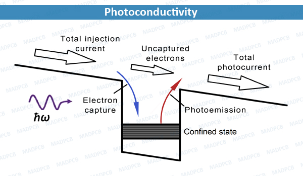
Photoconductivity
When light is absorbed by a material such as a semiconductor, the number of free electrons and holes increases, resulting in increased electrical conductivity. To cause excitation, the light that strikes the semiconductor must have enough energy to raise electrons across the band gap, or to excite the impurities within the band gap. When a bias voltage and a load resistor are used in series with the semiconductor, a voltage drop across the load resistors can be measured when the change in electrical conductivity of the material varies the current through the circuit.
Classic examples of photoconductive materials include:
- photographic film: Kodachrome, Fujifilm, Agfachrome, Ilford, etc., based on silver sulfide and silver bromide.
- the conductive polymer polyvinylcarbazole, used extensively in photocopying;
- lead sulfide, used in infrared detection applications;
- selenium, employed in early television and xerography.
Applications
- Photoresistor: when a photoconductive material is connected as part of a circuit, it functions as a resistor whose resistance depends on the light intensity. In this context, the material is called a photoresistor (also called light-dependent resistor or photoconductor). The most common application of photoresistors is as photodetectors, i.e. devices that measure light intensity. Photoresistors are not the only type of photodetector – other types include charge-coupled devices (CCDs), photodiodes and phototransistors – but they are among the most common. Some photodetector applications in which photoresistors are often used include camera light meters, street lights, clock radios, infrared detectors, nanophotonic systems and low-dimensional photo-sensors devices.
- Sensitization: Sensitization is an important engineering procedure to amplify the response of photoconductive materials. The photoconductive gain is proportional to the lifetime of photo-excited carriers (either electrons or holes). Sensitization involves intentional impurity doping that saturates native recombination centers having a short characteristic lifetime, and replacing these centers by new recombination centers having a longer lifetime. This procedure, when done correctly, results in an increase in the photoconductive gain after several orders of magnitude and is used in the production of commercial photoconductive devices. The text by Albert Rose is the work of reference for sensitization.
- Negative photoconductivity: Some materials exhibit deterioration in photoconductivity upon exposure to illumination. One prominent example is hydrogenated amorphous silicon (a-Si:H) in which a metastable reduction in photoconductivity is observable. Other materials that were reported to exhibit negative photoconductivity include molybdenum disulfide, graphene, indium arsenide nanowires, decorated carbon nanotubes, and metal nanoparticles.
- Magnetic photoconductivity: In 2016 it was demonstrated that in some photoconductive material a magnetic order can exist. One prominent example is CH3NH3(Mn:Pb)I3. In this material a light induced magnetization melting was also demonstrated thus could be used in magneto optical devices and data storage.
- Photoconductivity spectroscopy: The characterization technique called photoconductivity spectroscopy (also known as photocurrent spectroscopy) is widely used in studying optoelectronic properties of semiconductors.