What Is Polygon Pour?
A Polygon Pour is a group design object that is made up of simpler primitive objects. Polygon pours are used to create a solid or hatched (lattice) area on a PCB layer, using either Region objects or a combination of Track and Arc objects. Also referred to as copper pours, polygon pours are similar to a region except that they can fill irregularly shaped areas of a board as they automatically pour around existing objects, connecting only to objects on the same net as the polygon pour.
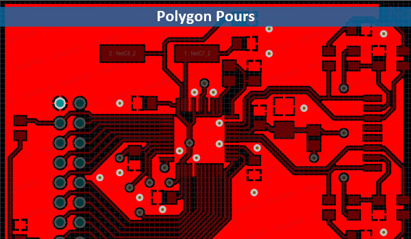
PCB Polygon Pours
On a signal layer, you can place a solid polygon pour to define an area for carrying large power supply currents, or as a ground-connected area for providing electro-magnetic shielding. Hatched polygon pours are commonly used for ground purposes in analog designs.
PCB designers have two choices when implementing large copper areas for power and ground regions: polygons or planes. Users often ask which is better for implementing power and ground nets, but both design features produce similar end results.
Polygons vs. Planes in Your PCB Layout
Polygons, also known as copper pours or polygon pours, are areas of the PCB that are filled or flooded with copper. This region is poured around existing components and traces, creating a region filled with copper hat has predefined clearance. Polygons should not be left floating and are generally tied back to a ground net to provide isolation. Polygons can only be placed on signal layers. Places polygons are commonly used include:
- surface layers containing placed components and routed traces
- internal signal layers containing routed traces and signal layers exclusively dedicated for power
- ground without any placed components or routed traces.
It can be difficult to identify which is better: a polygon or a plane. Polygons and planes can be used to implement a power and ground net distribution on a signal layer. If you’re restricted to a 2-layer stack-up only, polygons are the only solution to provide power and ground distribution throughout your board. When you’re designing a 4-layer or greater stack-up, you have a choice to use polygons on signal layers, planes on internal plane layers, or both.
Polygons on signal layers offer the best use of space. Because polygons are placed on signal layers, you can dedicate specific portions of a layer for power and ground distribution, rather than using an entire plane layer for power and ground planes. If dedicating numerous power and ground nets to specific layers, internal plane layers can be easier to work with and manage. The ability to divide or split an internal plane layer makes the creation and subsequent management of numerous and complex shapes easy and efficient.
Place Polygons with the Right CAD Tools
- Antennas, custom isolation structures, ground fill, and other RF structures are all examples of polygons in your PCB layout.
- You should carefully consider using polygon pour for padstack designs.
- You can create any polygon you need with a set of powerful CAD tools.
Create and Place Polygons with Advanced CAD Tools
CAD tools gives you multiple options for creating and placing polygon pours in your PCB layout. You have control over the size and shape of the pour, as well as whether it is solid or hatched. You can create these regions within a layer using high-quality CAD tools, or as a custom component. You also have control over polygon pour clearances and the size and shape of all copper features on your PCB. No matter what style of polygon or plane you need, you can create it in CAD tools.