What Is a Schottky Diode?
A Schottky Diode, also called as Hot-Carrier Diode, is a semiconductor diode formed by the junction of a semiconductor with a metal. It has a low forward voltage drop and a very fast switching action. When sufficient forward voltage is applied, a current flow in the forward direction. A silicon p-n diode has a typical forward voltage of 600-700mV, while the Schottky’s forward voltage is 150-450mV. This lower forward voltage requirement allows higher switching speeds and better system efficiency.
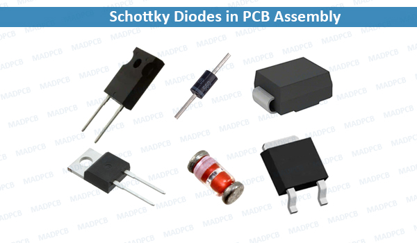
Schottky Diodes in PCB Assembly
The figure above show various types of Schottky diodes in printed circuit board (PCB) design and assembly. Any NPI or mass production projects concerning to circuit board layout, fabrication and assembly, feel free to contact MADPCB‘s professional sales engineers for quick quote, including flex PCB, rigid-flex board, thru-hole and HDI board. We have no bare PCB prototype MOQ, but have 5pcs PCB assembly prototypes.
It is named after the German physicist Walter H. Schottky (23 July 1886 – 4 March 1976).
How it Works?
A typical diode combines p-type and n-type semiconductors to form a p-n junction. In a Schottky diode metal replaces the p-type semiconductor. This metal can range from platinum to tungsten, molybdenum, gold, etc.
When metal is combined with an n-type semiconductor an m-s junction is formed. This junction is referred to as a Schottky Barrier. The behavior of the Schottky Barrier will differ depending on whether the diode is in an unbiased, forward-biased, or reverse-biased state.
- Forward-Biased State: Connecting the positive terminal of a battery to the metal and negative terminal to the n-type semiconductor will create a forward-biased state. In this state, electrons can cross the junction from n-type to metal if the applied voltage is greater than 0.2 volts. This results in a flow of current that’s typical for most diodes.
- Reverse-Biased State: Connecting the negative terminal of a battery to the metal and positive terminal to the n-type semiconductor will create a reverse-biased state. This state expands the Schottky Barrier and prevents the flow of electric current. However, if the reverse bias voltage continues to increase this can eventually break down the barrier. Doing so will allow current to flow in the reverse direction and may damage the component.
Application
- Voltage Clamping: While standard silicon diodes have a forward voltage drop of about 0.7 V and germanium diodes 0.3 V, Schottky diodes’ voltage drop at forward biases of around 1 mA is in the range of 0.15 V to 0.46 V, which makes them useful in voltage clamping applications and prevention of transistor saturation. This is due to the higher current density in the Schottky diode.
- Reverse Current and Discharge Protection: Because of a Schottky diode’s low forward voltage drop, less energy is wasted as heat, making them the most efficient choice for applications sensitive to efficiency. For instance, they are used in stand-alone (“off-grid”) photovoltaic (PV) systems to prevent batteries from discharging through the solar panels at night, called “blocking diodes“. They are also used in grid-connected systems with multiple strings connected in parallel, in order to prevent reverse current flowing from adjacent strings through shaded strings if the “bypass diodes” have failed.
- Switched-Mode Power Supplies: Schottky diodes are also used as rectifiers in switched-mode power supplies. The low forward voltage and fast recovery time leads to increased efficiency. They can also be used in power supply “OR”ing circuits in products that have both an internal battery and a mains adapter input, or similar. However, the high reverse leakage current presents a problem in this case, as any high-impedance voltage sensing circuit will see the voltage from the other power source through the diode leakage.
- Sample-and-Hold Circuits: Schottky diodes can be used in diode-bridge based sample and hold circuits. When compared to regular P-N junction-based diode bridges, Schottky diodes can offer advantages. A forward-biased Schottky diode does not have any minority carrier charge storage. This allows them to switch more quickly than regular diodes, resulting in lower transition time from the sample to the hold step. The absence of minority carrier charge storage also results in a lower hold step or sampling error, resulting in a more accurate sample at the output.
- Charge Control: Due to its efficient electric field control Schottky diodes can be used to accurately load or unload single electrons in semiconductor nanostructures such as quantum wells or quantum dots.
Schottky Diode Parameters
Below you’ll find a list of parameters to consider when choosing a Schottky diode for your next electronics project:
| Parameter | Description |
| Forward Voltage Drop | Any part specification will provide the forward voltage drop for a given current. The typical turn-on voltage for most Schottky diodes is around 0.2V. |
| Reverse Leakage Current | Increasing the temperature within a Schottky diode will significantly increase the reverse leakage current. This parameter is important to consider for preserving the integrity of your device. |
| Reverse Recovery Time | This parameter describes how much charge flows during the transition from an on to off state. This is usually measured in nano or picoseconds. |
| Reverse Breakdown | Look for parameters titled Peak Reverse Voltage, or Maximum Blocking DC Voltage to understand when your diode will allow current to flow in reverse. |
| Capacitance | The junction area within a Schottky diode has a small and capacitance is typically measured in picofarads. Capacitance will be defined at a given voltage in a spec sheet and is important for RF applications. |
| Working Temperature | A typical Schottky diode needs to maintain a junction temperature between 125 to 175℃. Keep this value in mind when working on heat distribution for your device. |
Designation
Commonly encountered schottky diodes include the 1N58xx series rectifiers, such as the 1N581x (1A) and 1N582x (3A) through-hole parts, and the SS1x (1A) and SS3x (3A) surface-mount parts. Schottky rectifiers are available in numerous surface-mount package styles.
Small-signal schottky diodes such as the 1N5711, 1N6263, 1SS106, 1SS108, and the BAT41–43, 45–49 series are widely used in high-frequency applications as detectors, mixers and nonlinear elements, and have superseded germanium diodes. They are also suitable for electrostatic discharge (ESD) protection of sensitive devices such as III-V-semiconductor devices, laser diodes and, to a lesser extent, exposed lines of CMOS circuitry.
Schottky metal–semiconductor junctions are featured in the successors to the 7400 TTL family of logic devices, the 74S, 74LS and 74ALS series, where they are employed as Baker clamps in parallel with the collector-base junctions of the bipolar transistors to prevent their saturation, thereby greatly reducing their turn-off delays.
Alternatives
When less power dissipation is desired, a MOSFET and a control circuit can be used instead, in an operation mode known as active rectification.
A super diode consisting of a PN-diode or Schottky diode and an operational amplifier provides an almost perfect diode characteristic due to the effect of negative feedback, although its use is restricted to frequencies the operational amplifier used can handle.