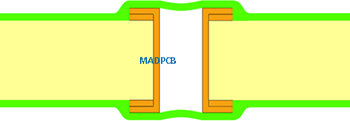
What’s Tented Via in PCB?
A Tented Via is defined as a via that is completely covered by the solder mask in printed circuit board. Tented vias are very popular because they have the lowest cost. Tenting can be used on a blind via or a thru-hole via. See Via Protection.
Vias under components are often tented to prevent the paste flux during PCB assembly from running into the holes and onto the opposite side of the circuit board, and to allow vacuum hold down on test equipment.

IPC-4761 Type I-a
IPC-4761 Type I-b
Vias Tenting Process
Tenting is normally done with a dry film solder mask rather than a liquid photo-imagable (LPI) solder mask. However, a single-pass LPI mask cannot guarantee 100% coverage of the vias. Obtaining the best possible via coverage with screen printing is a compromise between hole size, surface tension of the liquid mask and PCB thickness. Thru-hole vias can be tented on both ends to reduce chances of chemical entrapment during surface precleaning. However, be aware that trapped gas will expand inside the hollow via during reflow and might present reliability problems.
Concerns
A tented via which is open on one end may have another issue. This type of via can be subject to the “micro-etch” process. This is caused by a small amount of residual etchant trapped inside a tented via. This material will crystallize rapidly, creating copper sulfate crystals. Over time, these crystals can cause long term reliability issues. In the case of a electroless nickel immersion gold (ENIG) surface finish, the gold and small area of exposed copper near the tent could form a galvanic cell, accelerating the etch process.
Although tenting is inexpensive, other methods provide a more robust PCB design that does not suffer from the downsides of trapped gases or micro-etching. These factors must be carefully evaluated against the added processing cost of plugged vias which are much more reliable. Always discuss these options and considerations with your PCB fabricator before selecting any of these methods.