VIPPO/POFV is a method that resin plug vias first, and then copper plating over (cladded). Conventional technology is to separate POFV holes from non-POFV holes. Therefore, two electroplating processes are needed to ensure hole wall copper and cap and wrap plating copper thickness, the reduced amount of copper can not be too large. So, use the VIPPO process, of ten appear surface copper thickness exceeds the standard, copper thickness varies greatly, the outer etching difficult and cap copper thin and other problems, and the process is complicated, which adds difficulty to field operation.
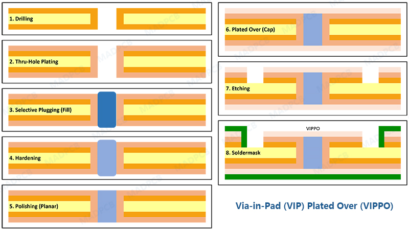
It consists of following steps in printed circuit board manufacturing:
- Drilling
- Through hole plating
- Selective plugging (fill)
- Hardening
- Polishing (planar)
- Plated over (cap)
- Etching
- Solder Mask
From the fabrication process, some people always describe VIPPO as vias capped to planar.
VIPPO Via-in-Pad Process
After many tests, data analysis, and defect analysis, different schemes for different quality defects have been formulated to verify, the research summarizes the improvement of each process, and obtains remarkable achievements.
MADPCB is good at making VIPPO/POFV backplane PCB and BGA board. Excepts for via-in-pad plated over, we suggest many other via protection processes.