What’s Voltage?
Voltage, electric potential difference, electric pressure or electric tension is the difference in electric potential between two points, which (in a static electric field) is defined as the work needed per unit of charge to move a test charge between the two points. In the International System of Units, the derived unit for voltage (potential difference) is named volt. In SI units, work per unit charge is expressed as joules per coulomb, where 1 volt = 1 joule (of work) per 1 coulomb (of charge). The old SI definition for volt used power and current; starting in 1990, the quantum Hall and Josephson effect were used, and recently (2019) fundamental physical constants have been introduced for the definition of all SI units and derived units. Voltage or electric potential difference is denoted symbolically by ΔV, simplified V, or U, for instance in the context of Ohm’s or Kirchhoff’s circuit laws.
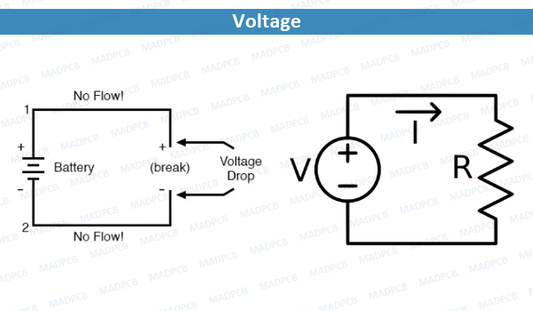
Voltage
Electric potential differences between points can be caused by the build up of electric charge (e.g., a capacitor), and from an electromotive force (e.g., electromagnetic induction in generator, inductors, and transformers). On a macroscopic scale, a potential difference can be caused by electrochemical processes (e.g., cells and batteries), the pressure-induced piezoelectric effect, and heat-induced electromotive force across metal-metal junctions. These latter processes at microscopic level have the physical origins previously mentioned.
A voltmeter can be used to measure the voltage (or potential difference) between two points in a system. Often a common reference potential such as the ground of the system is used as one of the points. A voltage can represent either a source of energy or the loss, dissipation, or storage of energy.
High-Voltage PCB Considerations
Have you ever seen electrical shocks and fires that occur on high voltage printed circuit boards (PCBs)? This is because of voltage spikes, which create a large potential difference between nearby conductive elements causing arcs through the air or shorts where the creepage or clearance distance has been effectively reduced or eliminated by dust or other debris. The resulting current can damage components, the board and pose a hazard to personnel. To reduce the possibility of these events, high voltage PCB design considerations, as listed below, should be implemented.
Designing circuit board that includes high voltages requires a different – and much more rigorous – approach than seen with other PCB designs. The need for more attention increases for high-density designs. Along with that approach, design teams also must become familiar with terminology that covers insulation, board materials, clearance, creepage, and altitude. Designers also should have an overall knowledge of regulations that can impact the circuit board.
High Voltage PCB Design and Manufacturing Tips
Here are some high voltage PCB design and manufacturing tips
- Choose appropriate creepage and clearance distance: Probably, the most design decision to minimize the probability of a high voltage hazard event is to route trace and place components and drill holes with adequate clearance and creepage distances. The IEC 60950-1 and/or UL-60950-1 standards provide guidance for these determinations.
- Avoid using sharp edged terminal pads: Using elliptical or circular pads is preferable to rectangular or square pads as they contribute to increased clearances.
- Select dielectrics and insulators: Using the comparative tracking index (CTI) to determine which material type work best for the specific application. The CTI is the maximum voltage measured in volts at which a material withstands 50 drops of contaminated water without forming conductive paths because of electrical stress, contamination, or humidity. Manufactures use the CTI to compare the performance of insulating materials under wet or contaminated conditions. Materials that have a high CTI value have a lower required minimum creepage distance and allow a shorter distance between two conductive parts. The shorter distance allows the use of high-density circuits in a high voltage environment. Besides, choosing high breakdown voltage materials is also important.
- Use the correct copper thickness and weight: It also assists with good high voltage circuit design. Thicker copper pathways withstand high currents and add physical strength to the board. Design teams should work with fabricators to ensure that the copper has a smooth, unblemished surface to prevent arcing.
- Utilize PCB surface finish: Protecting your circuit board during manufacturing is important. And you should employ the best surface finish for your design during fabrication to protect your circuit board from debris that may become trapped during board assembly and present a conductive target during operation.
- Apply conformal coating: Although sometimes omitted, having the right conformal coating type applied to your circuit board during the PCB assembly manufacturing stage should always be done for high voltage industrial boards to mitigate hazards and protect the PCB from environmental debris.
- Select appropriate components: high voltages rely on passives as well as active components. While design specifications for high voltage resistors may require low inductance and low temperature coefficients, ceramic capacitors must have high resistance, high temperature coatings and dielectrics that withstand high voltages. Capacitors used in high voltage circuits also should exhibit stable electrical parameters with a wide range of applied DC voltages and under different environmental conditions.