Table of Contents
Rigid PCB Profiling: Milling | Routing
PCB profiling involves either milling or v-scoring or the combination of both mechanical techniques. Milling, also referred to Routing, which is performed on a CNC mechanical machine with a routing tool. Routing is used to form the contours and breakouts of the PCB at the end of PCB manufacturing process when separate the individual PCBs from the production panel.
What we here mean with “milling” is a form of routing performed inside the PCB but not PCB design. Mechanical milling can be required to cut out the contour of a component, or to make room for any mechanical connection or for making slots, either NPTH or PTH in the PCB board.
PCB Milling Process
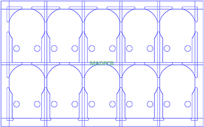
The final PCB manufacturing stage is to profile the printed circuit boards and cut them out of the production panel either by V-scoring or routing. For profiling, we use a computer-controlled milling machine or “router”. First the machine mills out any small slots or internal cut-outs. The cutter follows the routing path defined in the tool file. Next, the milling head automatically picks up a 2mm cutter, checks the diameter, and mills around each PCB. The brush around the milling head ensures that all the dust produced is collected by the vacuum system. The circuit boards are held in place by small bridges of material (routing-tab). We will drill through these and then remove each separate PCB from the production panel. This panel has also been V-scored.
Milling Mechanical Layer in Gerber Files
The mechanical layer date file should only contain the mechanical information for all layers that are necessary for your PCB board production. It must contain at least the following information:
- The exact board outlines, ideally including dimensions.
- Exact positions and sizes for all internal milling, slots or cutouts, ideally including dimensions.
It’s best practice to create the outlines using a small line- e.g. 0.5mm wide -where the center of the line represents the exact outline of the PCB board, cut-out or slot etc.
Notices:
- Without given dimensions, we will always take the center of the contour lines to be the exact outline of the board.
- Do not scale your mechanical layer, it should be 1:1 and reflect the exact dimensions of the PCB.
- In case of cut-outs or slots in your PCB, this layer is essential for the production process.
- The mechanical layer is (as for all layers) viewed from the top to the bottom through your PCB.
- Do not mirror or rotate the mechanical layer.
- Only include the relevant information in the mechanical layer area.
Milling Data
Do not provide actual routing or milling layers for PCB board contour or internal cut-outs. Routing and millings data is product specific and depending on the route tools, tool compensations, routing order, and direction used by the PCB fabricator. This means that we cannot use customer provided routing or milling data. We need to completely recreate them and this can lead to confusion or misinterpretations which may result in incorrectly routed PCBs. It’s our job as PCB manufacturers to prepare correct production routing and milling layers based on the information in your mechanical layer.
Milling parameters should follow as below,
| Parameter | Value |
| Min Milling tool diameter | 0.8mm |
| Min Radius for inner corners | 0.4mm |
| Min spacing copper/milling contour | 0.2mm |
Additional Milling Information
If required the additional information listed below should be included in your mechanical layer data.
- Reference Hole: The distance from one drill hole in X and Y to the PCB outline. This is particularly important when you only have NTPH holes without copper pads.
- Drill Position Symbols: Positional indication of all drills using symbols. Use different symbols from the drill map for each different drill size.
- PTH/NPTH indication: Indicate which holes and slots are PTH and which are NPTH.
- Customer Panels: If you provide panelized data include proper indications for break-routing and/or V-scoring.
- Layer Sequence: A clear layer sequence or buildup drawing for all copper, solder mask, and silkscreen layers. Include any additional layers such as peel-off or carbon. Provide the correct sequence as viewed from top to bottom and with the correct corresponding data file names.

