Table of Contents
Introduction of ENIG and ENEPIG
Nowadays, Electroless Nickel/Immersion Gold (ENIG) is commonly used for substrates that require soldering and mechanical contacting. Although ENIG with increased gold thickness (electroless gold) is a viable surface finish for gold wire bonding, presently electrolytic Ni/Au is still a widely used finish for this application since concerns still remain about issues with ENIG nickel corrosion and impact resistance.
However, electrolytic plating has its own challenges in meeting today’s requirements of weight and form factor that require finer lines and smaller pitch. Electroless plating is a more suitable finish for electronic parts as they continue down the path of smaller and lighter.
It is already established that Electroless Nickel/electroless palladium / Immersion Gold (ENEPIG) has excellent solderability for Sn-Ag-Cu based solders and forms high reliability wire bonds. ENEPIG is becoming the choice surface finish to meet present and future market demands.
In this paper, ENEPIG deposits were produced using commercially available chemicals to evaluate the reliability of lead free soldering and wire bond reliability as a function of palladium and gold deposit thicknesses. The data will show that high reliability soldering and bonding could be achieved on the same surface with a thickness of 0.02 to 0.1μm for palladium and as smaller as 0.2μm for gold.
Furthermore, solder joints and IMC formation for Sn-3.0Ag-0.5Cu and Sn-3.5Ag solders with ENIG and ENEPIG were studied. The solder joints were subjected to heat treatment at 150oC for a period of 1,000 hours. Subsequent analysis of the IMC showed that ENEPIG and ENIG showed the same IMC alloy formation with the Sn-3.0Ag-0.5Cu, while the IMC alloys formed with Sn-3.5Ag solders were different for ENIG as compared to ENEPIG.
Test Method
Two test vehicles were used in this study. Both were copper-clad laminate to which a 20μm thickness of electrolytic copper was plated. Table-1 shows this plating process.
To one of the test vehicles solder mask was applied and a solder mask defined 0.5mm BGA pattern was developed.
For IMC analysis, plating times were adjusted to produce plating deposit thickness of 5μm of Ni, 0.05μm of Pd, and 0.05μm of Au (Type F).
Table-1: Ni/Pd/Au Plating Process
|
Process |
Chemical | Temperature | Time |
|
Cleaner |
ACL-009 | 50 ºC | 5 min. |
| Soft etching | SPS type | 25 ºC |
1 min. |
|
Acid rinse |
10% H2SO4 | r.t. | 1 min. |
| Pre-dipping | 3% H2SO4 | r.t. |
1 min. |
|
Activator |
MNK-4 | 30 ºC | 2 min. |
| Electroless Ni | NPR-4 | 80 ºC |
25 min. |
|
Electroless Pd |
TPD-30 | 50 ºC | 5 min. |
| Electroless Au (F) | TSB-72 | 80 ºC |
12 min. |
| Electroless Au (A) | TWX-40 | 80 ºC |
25 min. |
Note:
- Different thickness was made by changed the dipping time.
- Electroless Au (F): For flash (thinner) gold.
- Electroless Au (A): For heavy (thicker) gold.
For study of the effects of different Pd and Au thickness, the Ni thickness was fixed at 5μm. The desired thicknesses of Pd and Au (type A) were then plated. Type A gold bath is capable of producing higher thicknesses of Au as compared to gold bath type F and was used for thicker gold deposits.
Results of Solderability Testing
Table 2 is a summary of the solderability test conditions which are considered severe assembly conditions. Fig-1 shows the results of this testing.
Table-2 ENEPIG Solderability Testing Conditions
| Solder Ball | Senju Sn-3.0Ag-0.5Cu 0.6mm⌀ |
| Flux | Senju 529D-1 RMA type |
| Reflow Instrument | TAMURA TMR-15-22LH |
| Reflow Condition | 5 times reflow at 260 deg. C top |
| Ball Pull Instrument | Dage series 4000 |
| Ball Pull Speed | 1000μm/sec |
|
Au Thickness (μm) |
||||||||||
|
0.03 |
0.05 | 0.07 | 0.1 | 0.15 | 0.2 | 0.25 | 0.3 |
0.4 |
||
| Pd Thickness (μm) |
0* |
5 | 20 | 20 | 10 | 10 | 13 | 10 | 8 | 5 |
| 0.01 | 90 | 90 | 90 | 90 | 90 | 80 | 80 | 55 |
60 |
|
|
0.02 |
100 | 100 | 100 | 100 | 100 | 90 | 90 | 90 | 90 | |
| 0.03 | 100 | 100 | 100 | 100 | 100 | 100 | 100 | 100 | 90 | |
| 0.05 | 100 | 100 | 100 | 100 | 100 | 100 | 100 | 100 |
98 |
|
|
0.07 |
100 | 100 | 100 | 100 | 100 | 100 | 98 | 95 | 90 | |
| 0.10 | 90 | 90 | 90 | 90 | 90 | 90 | 88 | 85 |
80 |
|
|
0.12 |
85 | 85 | 85 | 83 | 85 | 80 | 60 | 73 | 55 | |
| 0.15 | 50 | 50 | 60 | 60 | 55 | 55 | 55 | 60 |
50 |
|
|
0.20 |
50 | 60 | 50 | 55 | 58 | 70 | 30 | 35 | 30 | |
| 0.30 | 20 | 45 | 40 | 30 | 20 | 30 | 20 | 30 |
30 |
|
Fig-1 Results of Solderability Testing
Values in Fig-1 show a score for fracture mode after the completion of solder ball pull testing. Points were assigned to 3 types of fracture modes. For a complete fracture in the solder ball, 5 points were assigned. If the fracture interface showed <25% IMC it was assigned a point value of 2.5. Finally, a fracture that showed >25% IMC at the fracture surface was assigned zero points. For each test condition 20 balls were pulled and the 20 fractures surface were examined and assigned values as above. For example; if all 20 balls fractured completely in the solder with no IMC showing, each would be assigned 5 points for a total score of 100.
The calculation result indicates that solderability (for these severe test conditions) in case of palladium deposit thickness of 0μm, i.e., ENIG is less robust compared to that if only a small thickness of palladium is contained. However, as the palladium deposit thickness increases, it begins to show adverse effects on the fracture mode.
On the other hand increases in the gold deposit thickness (deposits up to 0.4μm) do not show a similar degradation on fracture mode. If solder joint reliability is the only consideration, a palladium deposit is the only consideration, a palladium deposit thickness of approximately 0.02 to 0.1μm and gold deposit thickness of approximately 0.05μm are more than adequate to achieve high reliability solder joints.
ENEPIG Gold and Palladium Deposit Thickness and Wire Bondability
In a previous paper, it was reported that ENEPIG deposits, when exposed to heat treatment could still prevent the diffusion of the underlying nickel, even in areas where the palladium deposit is extremely thin. Nickel diffusion to the gold surface is a major contributor to loss if bond strength.
The same test sample as those used for the solderability testing shown in Fig.-1 were used. Heat treatment at a temperature of 175oC for a period of 16 hours was completed before conducting the wire bonding testing under the conditions shown in Table-3.
Table-3 Wire Bonding Testing Conditions
| Wire | 1mil Gold |
| Capillary | B1014-51-18-12 (PECO) |
| Wire bonder | TPT HB16 |
| Stage temperature | 150 deg.C |
| Ultrasonic | 250mW(1st), 250mW(2nd) |
| Bonding time | 200m sec (1st), 50m sec (2nd) |
| Loading force | 25g(1st), 50g(2nd) |
| Step | 0.7mm (1st to 2nd wire length) |
| Wire pull instrument | Dage series 4000 |
| Wire pull speed | 170μm/sec |
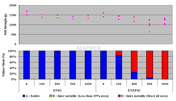
Fig.-2 shows the results of gold wire bond pull testing. The pull test data is the result of pulling 20 wires per each condition. Values shown in Fig.-2 are the average value of fracture strength obtained by the pull test.
As the results show at a palladium deposit thickness of 0μm, i.e. no palladium, a gold deposit thickness >0.3μm is required to obtain good wire bond values. In contrast, the wire bond strength for ENEPIG was higher even in areas with very low palladium deposit thickness. Further increase in palladium thickness did not improve the wire bond strength.
|
Au Thickness (μm) |
||||||||||
|
0.03 |
0.05 | 0.07 | 0.1 | 0.15 | 0.2 | 0.25 | 0.3 |
0.4 |
||
| Pd Thickness (μm) |
0* |
** | 4.3 | 4.4 | 3.9 | 3.8 | 3.7 | 5.1 | 8.6 | 9.1 |
| 0.01 | 6.8 | 7.9 | 7.9 | 8.1 | 8.7 | 8.6 | 9.6 | 10.6 |
10.5 |
|
|
0.02 |
6.7 | 7.9 | 8.6 | 8.2 | 8.5 | 9.0 | 9.5 | 10.2 | 10.7 | |
| 0.03 | 6.0 | 7.7 | 8.4 | 8.2 | 8.2 | 9.3 | 9.3 | 10.7 |
10.4 |
|
|
0.05 |
6.8 | 7.6 | 8.9 | 8.1 | 8.2 | 9.1 | 9.3 | 10.1 | 10.6 | |
| 0.07 | 7.0 | 7.8 | 8.1 | 8.3 | 8.8 | 9.5 | 9.1 | 10.9 |
11.1 |
|
|
0.10 |
6.0 | 6.7 | 8.1 | 8.3 | 8.4 | 9.3 | 9.2 | 10.0 | 10.8 | |
| 0.12 | 7.2 | 8.4 | 8.9 | 8.8 | 8.9 | 9.5 | 9.6 | 10.9 |
10.5 |
|
|
0.15 |
6.5 | 8.5 | 8.6 | 8.0 | 9.1 | 9.4 | 10.2 | 10.3 | 10.7 | |
|
0.20 |
6.0 | 8.8 | 8.9 | 8.7 | 9.1 | 9.4 | 10.0 | 10.3 |
10.5 |
|
| 0.30 | 6.6 | 8.8 | 8.5 | 8.3 | 9.0 | 9.6 | 10.0 | 10.2 |
10.6 |
|
Fig.-2 Results of Wire Bonding Testing
However, increasing the thickness of the gold deposit showed a marked improvement in wire bond strength. The palladium deposit thickness was fixed at 0.05μm to check the effect of gold deposit thicknesses of 0.05μm and 0.3μm, respectively.
Points with 6.5g wire pull strength in the gold deposit thickness of 0.05μm and those with 11.5g strength in the gold deposit thickness of 0.3μm were chosen, to conduct SEM observations on the secondary bond surface after the wire was pulled. Fig.-3 shows the results of these observations. Observation on the fracture surface indicated a wide difference between the 2 gold thicknesses tested. Exposed underlying metal was evident in the case of the 0.05μm gold thickness. In contrast with the 0.3μm gold thickness no exposed underlying metal was evident.
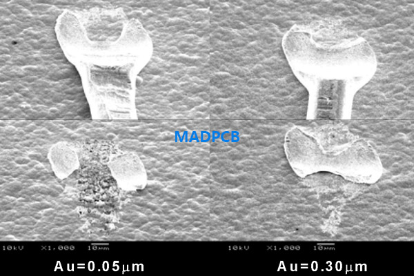
Gold Wire Bonding
Fig.-3 Difference in shape between secondary wire bond when making change to gold deposit thickness
Since god is a soft metal, it can be theorized that unless the gold deposit has a certain level of thickness for wire bonding, the underlying metal is scraped off to degrade the pull strength. The thicker gold deposit has a cushioning effect on the bond and produce a bond of superior strength. Insufficient gold and the possibility of nickel diffusion are the main contributors to the loss of wire bond strength.
Analysis of IMC Alloy Layers
As can be judged even from Fig.-1, the solder joint formed with ENEPIG maintain a high degree of reliability under strict reflow conditions compared to that of ENIG. Consequently, reflow was conducted at a temperature of 240oC as plated, and samples were also aged at 150oC for a period of 1,000 hours to simulate long-term reliability testing. In the previous paper, reliability evaluations were made on solder joints using Sn-3.0Ag-0.5Cu and Sn-37Pb solders. In this paper, however, we made evaluations on solder joint reliabilities using Sn-3.5Ag solder and showed the results in Fig-4. ENEPIG showed degradation in strength and fracture mode as heat treatment time elapses when sing Sn-3.5Ag solder, which was the same as that shown when using Sn-37Pb solder. In addition, like the previous paper, EPMA analysis was done of the distribution of each element at bonded interfaces after 1,000 hours of heat treatment at a temperature of 150oC. It turned out as shown in Fig.-5, that Sn-3.5Ag solder showed the same palladium aggregates that were observed with Sn-37Pb solder. In contrast when Sn-3.0Ag-0.5Cu is soldered to an ENEPIG deposit, the palladium at the IMC is uniformly distributed with no signs of aggregates. This absence of palladium aggregates with SAC solder is a possible reason why the solder joint reliability is higher than either Sn-37Pb or Sn-3.5Ag, under the conditions of testing.
The details of the IMC layers for Sn-3.0Ag-0.5Cu and Sn-3.5Ag were analyzed by TEM. Fig.-6 shows TEM image in the vicinity of IMC layers with Sn-3.0-0.5Cu soldered to the ENEPIG deposit after applying heat treatment at a temperature of 150oC for a period of 1,000 hours, and Fig.-7 shows the result of EDS analysis of the spots shown in the micrograph. According to the results of EDS measurement and diffraction measurement, Spot 3 is a layer referred to as the “phosphorous-rich layer” and assigned Ni3P+Ni. Spot 5 was assigned Ni-Sn-P since Ni, Sn and P were detected and no crystals were defined by diffraction. The Spots 6 and 7 had the same hexagonal crystal as that of Cu6Sn5 from the results of TEM diffraction measurement. In addition, since the EDS measurement result showed the detection of Ni, these spots were identified as (Cu, Ni)6Sn5. Furthermore, since this layer had uniform palladium distribution, the Spots were assigned as (Cu, Ni)6Sn5 + Pd. Subsequently, Sn-3.5Ag was soldered to the ENEPIG deposit, and we then conducted TEM and FE-SEM measurement of the IMC layers formed after aging at a temperature of 150oC for a period 1,000 hours. The results are shown in Fig.-8.
Solder Joint Reliability-1
Fig.-4 Results of Sn-3.5Ag Solderability Testing (Long-Term heat treatment testing at a temperature of 150oC)

Solder Joint Reliability-2
Fig.-5 Distribution of each element at bonded interfaces after heat treatment at a temperature of 150oC for a period of 1,000 hours, after mounting Sn-3.5Ag solder balls to ENEPIG deposit

IMC with Sn-3.0Ag-0.5Cu Soldered to ENEPIG Deposit
Fig.-6 TEM observation on IMC with Sn-3.0Ag-0.5Cu soldered to ENEPIG deposit after heat treatment applied at a temperature applied at a temperature of 150oC for a period of 1,000 hours
Quantitative Analysis Result (EDS); at %
|
Spot |
P | Ni | Cu | Pd | Sn |
| 3 | 28.7 | 68.7 | 0.4 | 0.0 |
2.1 |
|
5 |
18.0 | 64.2 | 0.1 | 0.0 | 16.8 |
| 6 | 0.0 | 18.9 | 33.2 | 0.6 |
47.3 |
|
7 |
0.1 | 17.2 | 35.1 | 1.1 |
46.4 |
Fig.-7 Results of EDS of TEM Image in Fig.-6
Applying long-term heat treatment under these conditions, two layers were found one was columnar and the other was of uniform crystal structure. The results of EPMA mapping (Fig.-5) show that the palladium aggregates were found only in the columnar alloy layer.
Further analysis were conducted on IMC Layer Spots 7 to 9 in the lower main part, the results of the EDS analysis shown in Fig.-9. Furthermore, from the diffraction results, we determined that the Spot8 was Ni-Sn-P layer, and the Spots 8 and 9 were Ni3Sn4 layers.
Subsequently, the diffraction result indicates that columnar parts (Spots 1 to 5) of the upper layer are of structure close to Ni3Sn4, while the EDS result indicates a ratio obviously different from that of Ni3Sn4. These ratio differences were observed with thick gold deposits where an alloy (Au, Ni)Sn4 was identified. Since AuSn4 and PdSn4 produce the same orthorhombic crystal and due to the element ratio of EDS, we determined this alloy as (Pd, Ni)Sn4. This (Pd, Ni)Sn4 alloy has portions that vary in palladium content.
The EPMA measurement in Fig.-5 showed the distribution of the palladium deposit thickness in alloy layers. Additional observations on the cross section of alloy layers with varying palladium thicknesses were conducted, The reflow process was conducted once at a temperature of 240oC and gave the results showed in Fig.-10. The results indicate that ENIG (Pd=0.00μm) has formed needle-lie ally layers and ENEPIG has formed uniform alloy layers. However, if the palladium deposit thickness is increased to 0.08μm or higher, the alloy layers become markedly thicker. The increased thickness has an adverse effect on the reliability of the solder joint.
Conclusion
TEM analysis was conducted on test pieces that were aged at a temperature of 150oC for a period of 1,000 hours after soldering Sn-3.0Ag-0.5Cu solder, an alloy layer (Cu,Ni)6Ni5 with even palladium distribution was identified as the main layer. On the other hand, Sn-3.5Ag solder, revealed a distinct columnar alloy layer (Pd,Ni)Sn4 on the uniform alloy layer Ni3Sn4. Consequently, it is believed that the presence of the alloy layer (Pd,Ni)Sn4 adversely affects solder joint reliability. In addition, it was found that solder joint reliability. In addition, it was found that solder joint reliability was more dependent on palladium deposit thickness than gold deposit thickness, and thereby it was essential to control the palladium deposit thickness.
On the other hand, with regard to wire bonding, it is indicated that the ENEPIG deposit makes it possible to control nickel diffusion to the deposit surface. In this paper, the palladium deposit and the gold deposit thickness were varied, to determine their role on wire bond strength. As a result, it was found that increased gold thickness has a cushioning effect and is more effective in enhancing the wire bond strength as compared to increasing the palladium thickness.
Summing up the study, solderability requires proper palladium deposit thickness, while thicker gold deposit is more advantageous for wire bondability. Increasing the gold thickness does not improve solder joint reliability, nor does increasing the palladium thickness improve wire bondability. Consequently, it was proved that controlling the palladium deposit thickness and the solder deposit thickness could be balanced to give high reliability for both soldering and wire bonding.
In recent years, electroless plating due to increasing reduction in weight and size of electronic parts has been getting attention in addition to lead-free soldering materials. With a good understanding of how the ENEPIG finish interacts with different lead free solders, ENEPIG can be the choice electroless alternative for today’s challenging electronic demands.
Fig.-8 TEM and FE-SEM observations on IMC with Sn-3.5Ag soldered to ENEPIG deposit after heat treatment applied at a temperature of 150oC for a period of 1,000 hours.

TEM and FE-SEM observations on IMC with Sn-3.5Ag soldered to ENEPIG
|
Spot |
P | Ni | Cu | Pd |
| 2 | 0.0 | 17.9 | 3.7 |
78.4 |
|
5 |
0.2 | 19.1 | 0.7 | 79.9 |
| 7 | 10.8 | 66.0 | 0.0 |
23.2 |
|
8 |
0.2 | 44.7 | 0.0 | 55.1 |
| 9 | 0.3 | 43.4 | 0.0 |
56.2 |
Fig.-9 Results of EDS of TEM Image in Fig.-8

Photograph of Alloy Layer
Fig.-10 Photograph of alloy layer after conducted the reflow process once at a temperature of 240oC on Ni-P/Pd/Au deposit with changed palladium deposit thickness.