Table of Contents
Staggered Microvias and Stacked Microvias PCB in HDI PCB
HDI printed circuit board (PCB) layers are piled up one by one using laser technology and plating technology after forming a conductor pattern on an insulating layer. Because wiring is possible on the connection part of each layer, this method achieves higher density and higher integration than ordinary multi-layer PCBs. So here you will learn about Staggered Microvias and Stacked Microvias PCB in HDI PCB. They are used for devices that require high-density wiring in a limited space.
Here are all about microvia I and microvia II in HDI PCBs using stacked microvias and staggered microvias.
Features of Staggered Microvias
- HDI PCBs with Staggered Microvia and Stacked Microvia
- Any combination with Laser Via, IVH or Plated Through Hole is possible
Applications of Staggered Microvias
- Cellular Phones
- Small Mobile Devices
- Car Navigation Systems
- Digital Cameras
- Digital Video Cameras
- Multi-functional Printers
Cross-Sections

Microvia I – Staggered Microvia
Microvia II – Stacked Microvia
Stack-ups

Microvia I Cross-section
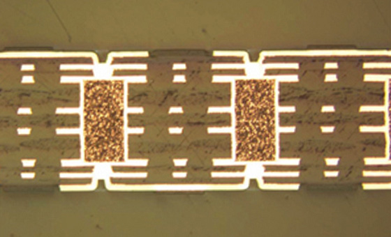
Microvia II Cross-section
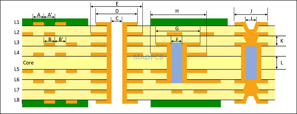
Design Rules
|
Parameter |
Symbol | Standard Spec |
Min Spec |
||
|
Trace Width/Spacing |
HDI Layer | A/A’ | 75/75 | 50/50 | |
| Core Layer | B/B’ | 75/75 |
50/50 |
||
|
Plated Through Hole |
Drill Diameter | C | 300 | 250 | |
|
Pad Diameter |
Outer Layer | D | 550 | 450 | |
| Inner Layer | E | 600 |
500 |
||
|
IVH (Inner Via Hole) |
Drill Diameter | F | 250 | 200 | |
| Pad Diameter |
Outer Layer |
G | 500 |
400 |
|
| Inner Layer | H | 500 |
450 |
||
|
Laser Via |
Via Diameter | I | 100 | 75 | |
| Pad Diameter | J | 250 |
220 |
||
|
Dielectric Thickness |
HDI Layer | K | 60 | 40 | |
| Core Layer | L | 100 |
60 |
||
* These figures are merely settings. They are subject to change without notice.
Click to know our PCB Capabilities and Fabrication Process.