Table of Contents
Types of PCB Materials: PCB Board Components and Understanding with Details
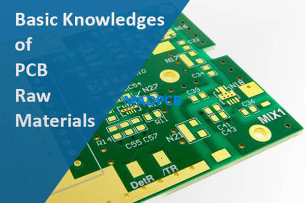
These are MADPCB internal technical data about basic knowledge about Types of PCB Materials this will be the PCB raw materials . The purpose is the understanding of the commonly used specifications and performance parameters of rigid PCB Copper Clad Laminate, Prepreg, Copper Foil, Solder Mask, and Silkscreen ink. Here I will discuss with details about Types of PCB Materials.
Here are almost all PCB materials with their details and pictures.
Prepreg
Prepreg (PP) is “pre-impregnated” composite fibers where a matrix material, such as epoxy, is already present.

PP Changing Process
- Main Function: as the matrix material among the inner layers of multilayer PCBs and is used to adjust the PCB thickness.
- Main Feature: The resin flows and cures in a certain pressure and temperature. The curving thickness differs from different PP model, which is used to adjust the PCB thickness.
- Storage: Constant Temperature (21+/-2°C), Constant Humidity (55+/-8%).
The resin in Prepreg (PP)
Resin type includes phenolic resin, epoxy resin, PTFE, polyimide (PI), triazine resin or/and bismaleimide and etc. The most commonly used is epoxy resin at present. Resin can be thermosetting material, which can happen macromolecule polymerization, with function and feature as following:
- Electrical insulation.
- As matrix material between copper foil and reinforcement material (glass fiber fabric).
- Feature: Electrically resistance, heat resistance, chemical resistance, water resistance.
E-Glass Fiber Fabric Specifications: 106, 1080, 3313, 2116, 7628
|
Specification |
Theoretical Thickness | RC (%) |
| 106 | 0.0513mm (2mil) |
72.5 |
|
1080 |
0.0773mm (3mil) | 66 |
| 3313 | 0.1034mm (4mil) |
57 |
|
2116 |
0.1185mm (5mil) | 54 |
| 7628 | 0.1951mm (8mil) |
46 |
Prepreg Sizes
Prepreg has standard sizes, including:
- 16”x18”
- 16”x21”
- 18’’x24”
- 12”x18”
- non-standard sizes can be customized
Copper Foil
- Main Function: be the conductive tracks on the top and bottom layer of a multilayer PCB.
- Main Feature: Cohered with PP at a certain pressure and temperature.
- Storage: Constant temperature and constant humidity.
The Classification of Copper Foil as per IPC-4562
|
Code |
Industrial Code | Metric | English | |||
| Basic weight
(g/m²) |
Nominal thickness(μm) | Basic weight
(oz/ ft²) |
Basic weight
(g/ in²) |
Nominal thickness (mil²) |
||
|
Q |
1/4oz(9μm) | 75.9 | 8.5 | 0.249 | 12.5 | 0.34 |
| T | 1/3oz(12μm) | 106.8 | 12.0 | 0.350 | 17.5 |
0.47 |
|
H |
1/2oz | 152.5 | 17.1 | 0.500 | 25.0 | 0.68 |
| M | 3/4oz | 228.8 | 25.7 | 0.750 | 37.5 |
1.01 |
|
1 |
1oz | 305.0 | 34.3 | 1 | 50.0 | 1.4 |
| 2 | 2oz | 610.0 | 68.6 | 2 | 100.0 |
2.70 |
|
3 |
3oz | 915.0 | 102.9 | 3 | 150.0 | 4.05 |
| 4 | 4oz | 1220.0 | 137.2 | 4 | 200.0 |
5.40 |
*We commonly used thickness including 1/3oz(12μm), 0.5oz, 1oz, 2oz, 3oz and 4oz.
Copper Clad Laminate
Copper clad laminate (CCL) is the main raw material of printed circuit boards, made of copper foil and PP in the certain temperature and pressure, with different thickness.
Classification by Resin
- Phenolic CCL (such as FR-2)
- Epoxy Resin CCL (FR-4, such as IT-180A)
- High Temperature Resistance CCL (such as FR-5)
- Polyimide CCL (such as PI, PET)
- Polytetrafluorethylene (PTFE or TEFLON) CCL (such as Taconic TLX-8)
- Bismaleimide Triazine (BT) CCL (such as Isola GI-180)
- Cyanide Ester (CE) CCL (such as CCL-HL950)
Classification of Copper Clad Laminates
|
Classification by Application |
Specifications |
Representation Material |
| Common CCL: FR-4 | Common Tg: ≥135℃ |
S1141 |
| Medium Tg: ≥145℃ |
S1141 150 |
|
| High Tg: ≥170℃ |
IT180A |
|
| High Frequency | High Performance FR-4 |
N4000-13 |
| PTFE |
Arlon RF-35 |
|
| Ceramic Filled (not PTFE) |
RO4350B |
|
| High Temperature Resistance | PI CCL |
Arlon 85N |
| Other Special Application | Halogen-free and CAF resistant |
S1155, IT180A |
Common FR-4 Copper Clad Laminates Parameter Table
|
Capability Property |
Standard | Typical Value of S1141 | Standard | Typical Value of IT158 | Standard |
Typical Value of IT180A |
|
IPC4101B |
/21 | /99 | /126 | |||
| Tg (°C) | ≥135 | 140 | 150-200 | 155 | ≥170 |
180 |
|
Td (°C) |
— | 310 | — | 345 | ≥340 | 345 |
| Dicy/PN | Dicy | PN |
PN |
|||
|
Filler |
No | Yes | Yes | |||
| Dk @1MHz | ≤5.4 | 4.6 | ≤5.4 | 4.8 | ≤5.4 |
4.8 |
|
Df @1MHz |
≤0.035 | 0.015 | ≤0.035 | 0.016 | ≤0.035 | 0.013 |
| CTE (Z axis) (50-260°C) | — | 4.5 | ≤3.5 | 3.3 | ≤3.0 |
2.8 |
|
T288 (min) |
— | 2 | ≥5 | 20 | ≥15 | 20 |
| Moisture Absorption | ≤0.8 | 0.15 | ≤0.5 | 0.08 | ≤0.5 |
0.1 |
Four Main Considerations of Selecting Copper Clad Laminates
- Processability
- Material Acquisition in Time
- Cost Factor
- The practicality of laws and regulations
Specific Aspects Upon Above Consideration Factors:
– Tg Value (consideration of Lead free);
– Td Value or T260, T288 (consideration of Lead free);
– Er (/Dk) and Tanδ (Dk and Df);
– Halogen Content (whether it is a halogen-free material);
– Other consideration aspects: CAF, IST, Q1000, UL level, CTI and moisture absorption.
Selecting Common Tg or High Tg CCL
- For common PCBs ≤ 10 layer, and the finished copper of inner and outer layer ≤ 2 oz,
- Material Selection: S1141, S6018 (RCC) (common Tg)
To meet one of the following conditions, material selection: IT180A, LDPP (high Tg)
- As per Acceptance Standards of Nation and Military;
- The finished copper thickness of inner and outer layer ≥ 3 oz;
- Layer Count ≥ 12 layer;
- The finished PCB thickness ≥ 3.0mm;
- The high-density heat dissipation hole distance < 1.2mm after hole diameter compensated.
High Frequency PCB CCL Selection
- Dk (/Er): it’s up to specific circuit design and function, which has directly effect on PCB stack-up structure, especially for PCB thickness and impedance control; (Signal transfer rate is inversely proportional to the square of Er. Lower Dk PCB has faster transfer rate.)
- Df: generally, wish the smaller Df, the better. The Df stands for signal loss in the PCB circuit;
- Variation in thickness: the substrate is mainly determined to characteristic impedance, and affects signal interference between the layers;
- The Dk consistency of the up and down dielectric of the signal tracks;
- Material Processability;
- TCK of dielectric constant.
Soldermask & Silkscreen Inks
- Soldermask provides solder resist and protection for conductor
- Silkscreen acts as identification role
Ink Properties
|
Chemical Properties |
Solder Mask Ink Electrical Properties |
Silkscreen Ink Properties |
|
|
|
Commonly Used Solder Mask Color

Common Soldermask Color
Ink Acceptance Common Criteria

Ink Acceptance Common Criteria