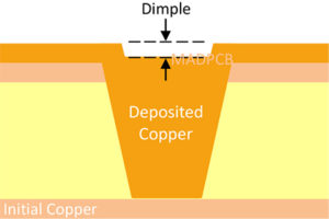
Equation: Dimple= A – B
In HDI PCB manufacturing, Blind Microvia (BMV) Fill is an important process to achieve planar surfaces to (1) allow reliable formation of sequent layers with a minimum amount of copper deposited onto the surface to improve fine-line yield; (2) allow better SMD soldering, especially for big size BGAs.
Acceptance Criteria for Cap Plating of Filled Vias as per IPC-A-600:
Target condition: Copper surface is planar with no protrusion (bump) and/or depression (dimple)
Acceptable condition – Class 1,2, and 3:
• Separation of copper cap to fill material
• No separation of the cap plating to underlying plating
• Cap protrusion (bump) and/or depression (dimple) meets the dimensional requirements in IPC 6012
• Fill material within the blind via shall be planar with the surface within +/- 76μm (3mil) unless otherwise specified
• When cap plating is specified, fill material within the blind via shall meet the dimple/bump requirements of IPC 6012
• No voids in the cap plating over the resin fill
Through the use of vacuum tables and power squeegees, we have been able to fill up blind vias or microvia to 10:1 aspect ratio vias with no voiding, or to say, no dimple in the vias. Many of PCB fabricators produce via-in-pads too infrequently to invest in equipment to planarize boards with the sufficient throughput and quality required for PCB Assembly. MADPCB facility is equipped with conveyorized planarizer that utilizes ceramic scrubbing rollers to ensure a high grade surface finish for via-in-pad applications. With its assistance, the copper reduction thickness can be controlled as thin as 2μm per polishing time no matter rigid or flex circuits.

