Table of Contents
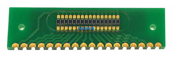
Half-hole PCB Boards Processing principle:
Either drilling or milling process, the rotation direction of SPINDLE is clockwise. When the machining tool reach point A, the hole wall copper layer of point A are closely linked with base layer, which avoid hole wall separated from the copper layer when extension, and the same time make assure no copper crooked and residue. While machining tool reach point B, because of copper attached to the hole wall, with no support of A schematic diagram, the tool forward running, the copper layer will curl with the cutter rotating under the external force to produce copper stab tilt, residues.
Processing Problems
Generally, there are 4 types plated half-hole printed circuits, which suitable for two ways:
- Type I and II are large plated half-hole spacing electronic circuits, second milling on the positive and negative: Due to half hole spacing of these two types castellated circuits board is bigger than 3mm, first milling process could complete CS layer half hole plating, and then the second milling process will complete SS side plating. In the positive and negative processing, PCB board edge with two different separate stress points. The finished half-plated-hole is smooth and tidy by this way. This way is also relatively simple and easy to guarantee the quality.
- Type III and IV edge plated PCB are with the diameter of half hole less than 0.8mm, and spacing of the center between two holes is about 1mm, and the space of two adjacent rows no bigger than 2.5mm. For the processing of these types printed circuit board, we need to consider space of each half-hole and part of two sides. If it encounters following problems, there may appear micro connection problem.
Problem Analysis
Design
In the original design, half-plated hole space is only 0.56mm, and pad clearance of each half hole is only 0.15mm. In the fabrication process, the cutter cuts hole edge directly, when the cutter wearing, the pads may be flanging. At the same time, the pad space is too small, which will cause failure micro-connection of pads.
Improved design: change the two rows cooper connection as hole ring and increase 0.05mm to space of half-hole pad pitch. And in order to ensure the width of half plated hole the same time, we do the following improvement: reduce pads width 0.025mm only for Half-Moon Through Hole pad parts close to (B position), keep the width of rest of the pad, which could ensure the pad pitch increase to 0.20mm (C position).
Support PCB
As the half hole is drilled on the PTH edge, the half hole of the bottom circuit board may with hole flanging if there is no enough support when the drill bit drilling. So the bottom PCB board using in the second drilling could not be ignored. It must be changed after each second drilling to make sure enough support for drilling and reduce the copper side flips.
Choose the Drill
Normal drill bit may appear biased drilling, break when drilling the PTH hole, slot drill is more suitable for processing such circuit board.
If the second drilling made as the whole PCB board processing, there may be irregular harmomegathus, which will lead to inconsistent for each array.
Improvement Measures
In order to avoid irregular harmomegathus in the production lead to the inconsistency of each array after second drilling, the producing process flow nee to adjust:
- Original process: Sawing →inner layer →lamination →drilling →PTH →plating →outer layer →solder mask → silkscreen →ENIG →second drilling →profile
- Improved process: Sawing →inner layer →lamination →drilling →PTH →plating →outer layer →solder mask →silkscreen →ENIG →first machining (outer profile) →second drilling →second machining (inner tank)
If using a single plated through half-hole PCB processing secondary drilling and secondary machining after process changes, the operation time for putting up and down PCB board will increase. In order to reduce operation time, we use second drilling combination panel, that is design it as single PCB compensation, re-panelizing according to the requirement, every time to put up PCB is still the original imposition PCB board. Because it is single PCB board compensated output data, it could avoid inconsistency due to printed PCB material irregular harmomegathus.
Result of Implementation
The quality of half-hole plating achieves desired level through improvement in design principle, PCB manufacturing processes and optimization of processing methods, which assure the final quality of half PTH hole circuit PCB. And the four corners and the middle of whole circuit board keep the same.


