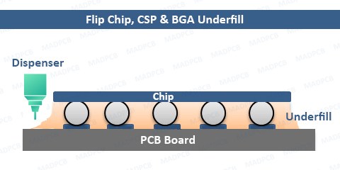
Apply Process:
- Dispensing the liquid thermoset epoxy by a dispenser.
- The epoxy will capillary flow into the gaps between chip and PCB.
- Heat-up the PCB assemblies to cure the epoxy till to dry.
The cured underfill, with about 1mil (25mircon) gap between chip’s bottom side and the PCB’s top side, encapsulates the bottom side of the silicon chip, covering the fragile interconnected pads between the chip and PCB. Underfill provides a strong mechanical bond between the chip and the PCB’s connection, protecting the solder joints from mechanical stress. It helps transfer heat, and also softens the mismatch between the coefficient of thermal expansion (CTE) between the chip and the board.
Underfill is commonly used for ball grid array (BGA) based storage for applications such as handheld devices, which must pass drop or tumble tests. When a BGA device is exposed to repeated heating and cooling cycles, a BGA chip will expand or contract at a different rate than that of the underlying substrate, due to the difference in each material’s coefficient of thermal expansion. This differential creates mechanical stress on the device’s solder joints.
Underfill is used as a stress relieving agent, evenly distributing the expansion and contraction effects. By spreading stresses throughout the chip and PCB interface with a mechanical bond, less stress is concentrated on the solder joints, increasing device reliability.

