Table of Contents
Back Drilling
Plated through holes (PTH) are electrically connect two or more PCB copper layers together, and serve as conventional connecting points for traces and components throughout a multilayer printed circuit board. But sometimes no need the via with whole barrel. The unused portion of the PTH that serves no functional purpose to the circuit is called a stub.
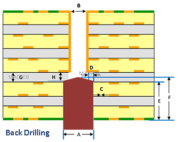
Back Drilling, also known as Controlled Depth Drilling (CDD), is a technique used to remove the unused portion, or stub of copper barrel from a thru-hole in a PCB board. When a high-speed signal travels between copper layers through a copper barrel, it can be distorted. If the signal layer usage results in a stub being present, and the stub is long then that distortion can become significant.
Backplanes and thick circuit boards in particular, can endure significant signal integrity disturbances through stubs. For high frequency PCBs (e.g. with controlled impedance), the application of back drilling, as well as the application of blind and buried vias, can be part of the solution.
Controlled depth drilling can be applied any type of printed circuit board where stubs cause signal integrity degradation, with minimal design and layout considerations. In contrast, when using blind vias, the aspect ratio has to be kept in mind. These stubs can be removed by re-drilling those holes after PCB fabrication is complete, with a slightly larger drill. The holes are back drilled to a controlled depth, close to but not touching the last layer used by that via.
Advantages of Back Drilling:
- Reduced deterministic jitter
- Lower Bit error rate (BER)
- Less signal attenuation with improved impedance matching
- Increased channel bandwidth
- Increased data rates
- Reduced EMI radiation from the stubs
- Reduced excitation of resonance modes
- Aspect ratio can be neglected (in contrast to blind vias)
Back Drilling Design Values
|
Index |
Type |
Value min. |
|
A |
Back drilling Ø |
400µm |
|
B |
Plated-through via Ø | 200µm |
| C | Copper clearance |
150µm |
|
D |
Ø-Difference circumference | 100µm |
| E | Back drilling depth |
200µm |
|
F |
Distance to connected layer | see below |
| G | Thickness target layer |
see below |
|
H |
Thickness stub remainder (safety) |
see below |
Required target layer thickness “G”
If you need a special layer buildup, please keep to the following min. prepreg thickness of the layer in which the drilling stops (G). If you do not need a special layer buildup, we will do all the necessary thickness calculations regarding the thickness of “G”.
| F ≤ 1.0mm | 1.0mm < F ≤ 2.0mm | 2.0mm < F ≤ 3.0mm | 3.0mm < F ≤ 4.0mm | |
| G min. | 250µm | 300µm | 400µm | 500µm |
| H | 125µm | 150µm | 200µm | 250µm |
| Tolerance | ± 100µm | ± 125µm | ± 175µm | ± 225µm |

