Table of Contents
Edge Plating | Castellation | Sideplating
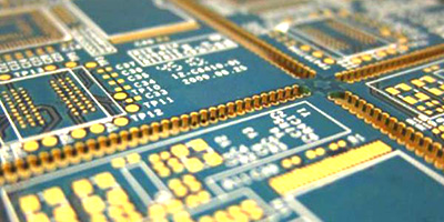
Edge Plating in PCB industry, sometimes referred to as Castellation or Sideplating, is a great way to ensure a strong connection through your printed circuit board and reduce the chance of board failures that can be costly to remedy. The surface finish of edge plating can be ENIG, ENEPIG, HASL and others if it can provide electrical connections. With sideplating, the printed circuit board (PCB) edge is used for technical features of the later PCB assembly.
Definition of Edge Plating?
There is no definition of edge plating per IPC standards. Although, edge plating is generally accepted as being copper plating that continue from the top to the bottom surfaces of a PCB board and along at least one of the perimeter edges. The copper plated edge allows for electric conduction, and space creates opening for mounting multiple boards or embedding edge connectors.
How to Design Edge Plated PCB?
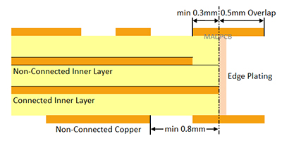
To guarantee the manufacturability of the edge plating, the metallized area must be defined using overlapping copper (copper surface, pads, or traces) in the layout file.
- Minimum overlap is 0.50mm.
- On the connected layer, minimum 0.30mm of connected copper must be defined.
- On non-connected layers, the copper should have a gap of minimum 0.80mm from the outer contour.
How to Define Edge Plating?
Have you ever designed edge plating board? When meet a project requires slideplating PCB, some PCB designers don’t know how to define it in their Gerber files, or convey this requirement to the PCB fabricator. At MADPCB, we provide technical support at the front-end CAM during edge plating PCB design.
How to define it? Make sure there is an anchor strip along the external top and bottom edges, and any plane(s) (may have) that connect to the slideplating extend out the edge and having a callout on the fab drawing that points to the relevant edge(s) that states something like:
- Slideplating indicated area using X Oz copper. Deburr and break sharp edges.
- With the addition to the note of something along the following if there is/are any plane(s) that connect to it.
- XXX plane on layer(s) N (and N) must connect to the edge plated area(s).
Metalized Edge Plating Fabrication Process
- Drilling -> Milling Metal Slot -> Get Rid of Dirt -> Copper Electroless
The outer contours, to be metallized, must be milled before through-hole plating process, as the metallization of the edges take place during this fabrication step. After the deposition of copper, the intended surface finish is finally applied to the edges.
- Fabrication Issues:
- Copper Peeling -Plating over a large substrate surface can lead to the plated copper peeling due to a lack of adhesion strength. We address this by first roughening the surface through a combination of chemical and other proprietary means. Next, we employ direct metallization, which has a higher copper bond strength, to prepare the surface for plating.
- Burrs -Often edge plating, especially on castellation holes, can result in burrs from the final machining process. We apply a modified, proprietary process flow that results in the burrs being polished down to the edge of the feature.
- Fab Note:
- The antenna position of the gold pad is too large, affecting customer soldering or signal transmission.
- The inner edge pad is connected to the wires on the board, resulting in a short circuit.
- The stamp hole is designed at the edging groove and must be handled in the 2nd drilling process.
- Through the process-related manufacture of the individual PCBs as a panel, a continuous metallization of the outer edges is not possible. No metallization can be applied where the small panel bridges are located.
- One request, the slideplating metallization can be covered with solder mask.
- When purchasing edge plating boards, you must confirm with your PCB supplier the possibility of manufacturing PCBs with plating process, and extent to which the fabricator can edge plate the PCB. Your Gerber files or fab drawing should indicate in a mechanical layer where they need slideplating, and the surface finish they need on it. Most manufacturers prefer a selective ENIG as the only surface finish suitable for round castellation.
Benefits of Edge Plating
It can improve the quality and reliability of your circuit boards through delivering improved current conduction in a board. He right level of conduction is essential for components to be able to operate in the way they were designed to. It can also help to protect more vulnerable edge connections.
But there are more benefits to the performance of your printed board when it’s edge plating.
- Thermal Distribution: One of the key benefits of edge plating is its ability to support thermal distribution. Similar to thermal vias, when components become overheated, they are more likely to fail, causing potentially critical damage to the board itself. As customers design circuit boards with more capabilities, using more components tightly packed onto smaller boards, effective thermal distribution becomes essential to channel excessive heat away from temperature-sensitive components. Without the ability to escape, the heat will compromise the performance and reliability of the board.
- Signal Integrity: Edge plating can also improve signal integrity. Signal integrity is becoming more important as PCB boards are becoming more complex, demanding faster connections and more complex layouts. Plating on PCB edge is fairly straight forward process in terms of the equipment required, though the process sequence can vary.
Edge Plating PCB Applications
It has a variety of purposes, such PCBs are commonly applied in many industries including, but not limited to:
- Edge Soldering
- Board-to-Board Connection
- Increase Current Carrying Capacity
- Housing Connection
- Improvement of EMC Performance


