What is a Ferrite Bead?
A Ferrite Bead is a passive device that filters high-frequency noise energy over a broad frequency range. It becomes resistive over its intended frequency range and dissipates the noise energy in the form of heat. The ferrite bead is connected in series with the power supply rail and is often combined with capacitors to ground on either side of the bead. This forms a low-pass filter network, further reducing the high-frequency power supply noise.
An effective method for filtering high-frequency power supply noise and cleanly sharing similar voltage supply rails (that is, analog and digital rails for mixed-signal ICs) while preserving high-frequency isolation between the shared rails is the use of ferrite beads.
However, improper use of ferrite beads in system design can lead to some detrimental issues. Some examples are unwanted resonance due to combining the bead with a decoupling capacitor for low-pass filtering and the effect of DC bias current dependency that degrades the EMI suppression capability of the bead. With proper understanding and consideration of the ferrite bead’s behavior, these issues can be avoided.
This page discusses the important considerations that system designers need to be aware of when using ferrite beads in power supply systems such as impedance vs. frequency characteristics with varying DC bias current and unwanted LC resonance effects. Ultimately, to address the issue on the unwanted resonance, damping techniques will be introduced and a comparison of the effectiveness of each damping method will be presented.
The device used to demonstrate the effects of ferrite beads as an output filter is a 2 A/1.2 A DC-to-DC switching regulator with independent positive and negative outputs (ADP5071). The ferrite beads used in the article are mainly chip-type, surface-mount packages.
Ferrite Bead Simplified Model and Simulation
A ferrite bead can be modeled as a simplified circuit consisting of resistors, an inductor, and a capacitor. RDC corresponds to the DC resistance of the bead. CPAR, LBEAD, and RAC are (respectively) the parasitic capacitance, the bead inductance, and the AC resistance (AC core losses) associated with the bead.
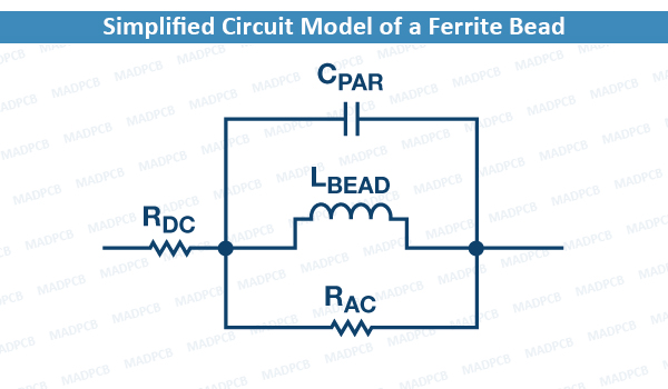
Simplified Circuit Model of a Ferrite Bead
Ferrite beads are categorized by three response regions: inductive, resistive, and capacitive. These regions can be determined by looking at a ZRX plot, where Z is the impedance, R is the resistance, and X is the reactance of the bead.
To reduce high-frequency noise, the bead must be in the resistive region; this is especially desirable for electromagnetic interference (EMI) filtering applications. The component acts like a resistor, which impedes the high-frequency noise and dissipates it as heat. The resistive region occurs after the bead crossover frequency (X = R) and up to the point where the bead becomes capacitive. This capacitive point occurs at the frequency where the absolute value of capacitive reactance (–X) is equivalent to R.
In some cases, the simplified circuit model can be used to approximate the ferrite bead impedance characteristic up to the sub-GHz range.
The Tyco Electronics BMB2A1000LN2 multilayer ferrite bead is used as an example. Figure below shows the measured ZRX response of the BMB2A1000LN2 for a zero DC bias current using an impedance analyzer.
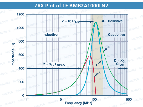
ZRX Plot of TE BMB2A1000LN2
For the region on the measured ZRX plot where the bead appears most inductive (Z ≈ XL; LBEAD), the bead inductance is calculated by the following equation:
Lbead = XL/2πf (1)
where f is the frequency point anywhere in the region the bead appears inductive. In this example, f = 30.7 MHz. XL is the reactance at 30.7 MHz, which is 233 Ω.
Equation 1 yields an inductance value (LBEAD) of 1.208 µH.
For the region where the bead appears most capacitive (Z ≈ |XC|; CPAR), the parasitic capacitance is calculated by the following equation:
CPAR = 1 / (2πf x |XC|) (2)
where f is the frequency point anywhere in the region the bead appears capacitive. In this example, f = 803 MHz |XC| is the reactance at 803 MHz, which is 118.1 Ω.
Equation 2 yields a parasitic capacitance value (CPAR) of 1.678 pF.
The DC resistance (RDC), which is 300 mΩ, is acquired from the manufacturer’s data sheet. The AC resistance (RAC) is the peak impedance where the bead appears to be purely resistive.
Calculate RAC by subtracting RDC from Z. Because RDC is very small compared to the peak impedance, it can be neglected. Therefore, in this case, RAC is 1.082 kΩ.
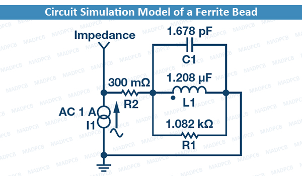
Circuit Simulation Model of a Ferrite Bead
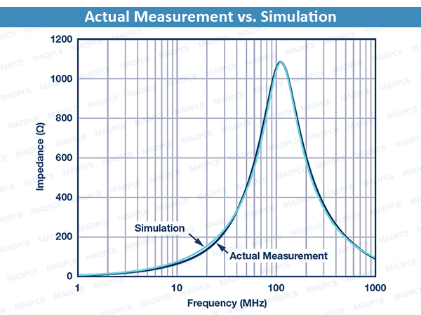
Actual Measurement vs. Simulation
The ferrite bead model can be useful in noise filtering circuit design and analysis. For example, approximating the inductance of the bead can be helpful in determining the resonant frequency cutoff when combined with a decoupling capacitor in a low-pass filter network.
However, the circuit model specified in this article is an approximation with a zero DC bias current. This model may change with respect to DC bias current and, in other cases, a more complex model is required.
DC Bias Current Considerations
Selecting the right ferrite bead for power applications requires careful consideration not only of the filter bandwidth but also of the impedance characteristics of the bead with respect to DC bias current. In most cases, manufacturers only specify the impedance of the bead at 100 MHz and publish datasheets with frequency response curves at zero DC bias current. However, when using ferrite beads for power supply filtering, the load current going through the ferrite bead is never zero and, as DC bias current increases from zero, all of these parameters change significantly.
As the DC bias current increases, the core material begins to saturate, which significantly reduces the inductance of the ferrite bead. The degree of inductance saturation differs depending on the material used for the core of the component. Figure below shows the typical DC bias dependency of the inductance for two ferrite beads. With 50% of the rated currents, the inductance decreases by up to 90%.
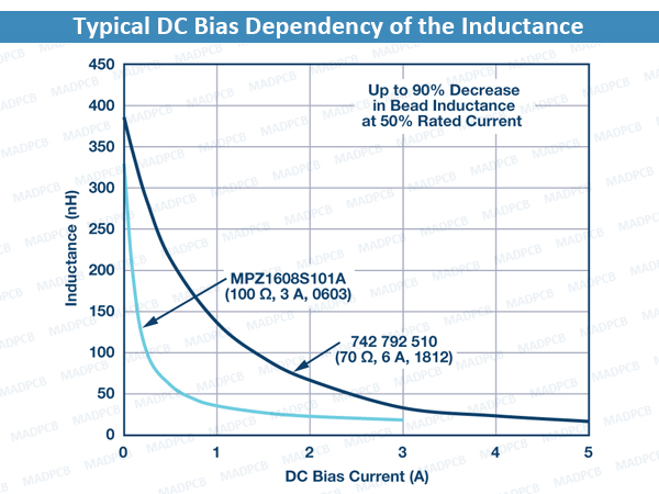
Typical DC Bias Dependency of the Inductance
For effective power supply noise filtering, a design guideline is to use ferrite beads at about 20% of their rated DC current. As shown in these two examples, the inductance at 20% of the rated current drops to about 30% for the 6 A bead and to about 15% for the 3 A bead. The current rating of ferrite beads is an indication of the maximum current the device can take for a specified temperature rise and it is not a real operating point for filtering purposes.
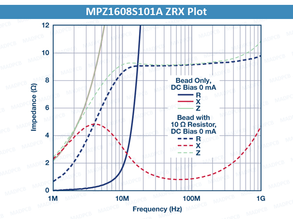
In addition, the effect of DC bias current can be observed in the reduction of impedance values over frequency, which in turn reduces the effectiveness of the ferrite bead and its ability to remove EMI. The following 2 figures show how the impedance of the ferrite bead varies with DC bias current. By applying just 50% of the rated current, the effective impedance at 100 MHz dramatically drops from 100 Ω to 10 Ω for the TDK MPZ1608S101A (100 Ω, 3 A, 0603) and from 70 Ω to 15 Ω for the Würth Elektronik 742 792 510 (70 Ω, 6 A, 1812).
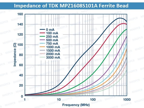
Impedance of TDK MPZ1608S101A Ferrite Bead
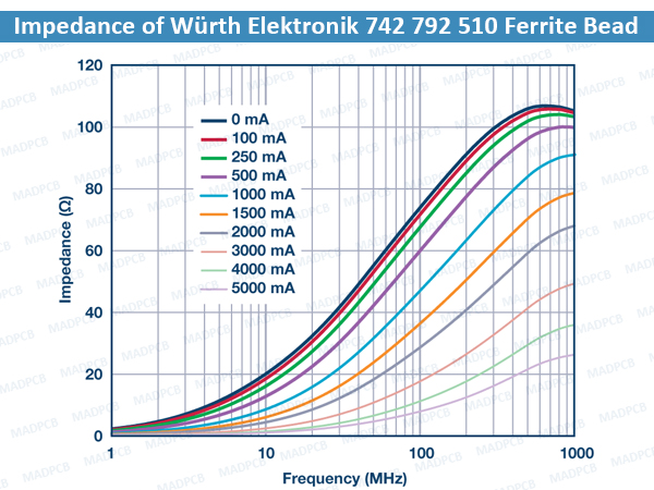
Impedance of Würth Elektronik 742 792 510 Ferrite Bead
System designers must be fully aware of the effect of DC bias current on bead inductance and effective impedance, as this can be critical in applications that demand high supply current.
LC Resonance Effect
Resonance peaking is possible when implementing a ferrite bead together with a decoupling capacitor. This commonly overlooked effect can be detrimental because it may amplify ripple and noise in a given system instead of attenuating it. In many cases, this peaking occurs around the popular switching frequencies of DC-to-DC converters.
Peaking occurs when the resonant frequency of a low-pass filter network, formed by the ferrite bead inductance and the high Q decoupling capacitance, is below the crossover frequency of the bead. The resulting filter is underdamped.
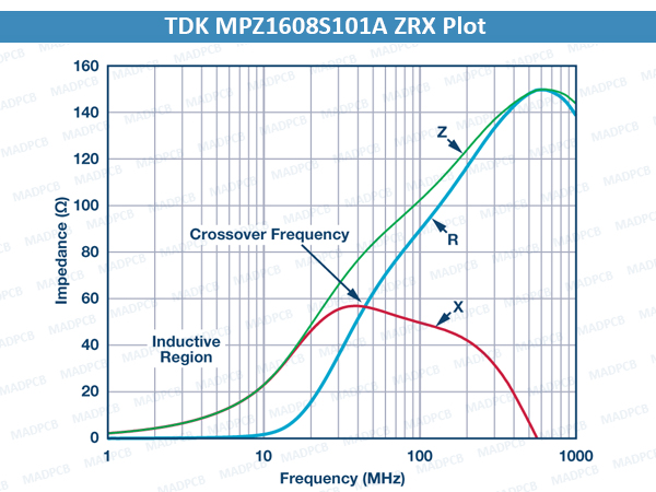
TDK MPZ1608S101A ZRX Plot
The figure above shows the measured impedance vs. frequency plot of the TDK MPZ1608S101A. The resistive component, which is depended upon to dissipate unwanted energy, does not become significant until reaching about the 20 MHz to 30 MHz range. Below this frequency, the ferrite bead still has a very high Q and acts like an ideal inductor.
LC resonant frequencies for typical bead filters are generally in the 0.1 MHz to 10 MHz range. For typical switching frequencies in the 300 kHz to 5 MHz range, additional damping is required to reduce the filter Q.
As an example of this effect, Figure below shows the S21 frequency response of the bead and capacitor low-pass filter, which displays a peaking effect. The ferrite bead used is a TDK MPZ1608S101A (100 Ω, 3 A, 0603) and the decoupling capacitor used is a Murata GRM188R71H103KA01 low ESR ceramic capacitor (10 nF, X7R, 0603). Load current is in the microampere range.
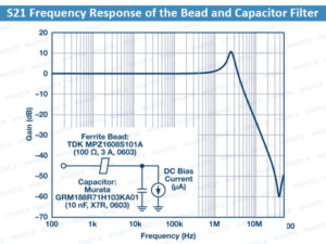
S21 Frequency Response of the Bead and Capacitor Filter
An undamped ferrite bead filter can exhibit peaks from approximately 10 dB to approximately 15 dB depending on the Q of the filter circuit. The peaking occurs at around 2.5 MHz with as much as 10 dB gain.
In addition, signal gain can be seen from 1 MHz to 3.5 MHz. This peaking is problematic if it occurs in the frequency band in which the switching regulator operates. This amplifies the unwanted switching artifacts, which can wreak havoc on the performance of sensitive loads such as the phase-lock loop (PLL), voltage-controlled oscillators (VCOs), and high resolution analog-to-digital converters (ADCs).
The result has been taken with a very light load (in the microampere range), but this is a realistic application in sections of circuits that need just a few microamperes to 1 mA of load current or sections that are turned off to save power in some operating modes. This potential peaking creates additional noise in the system that can create unwanted crosstalk.
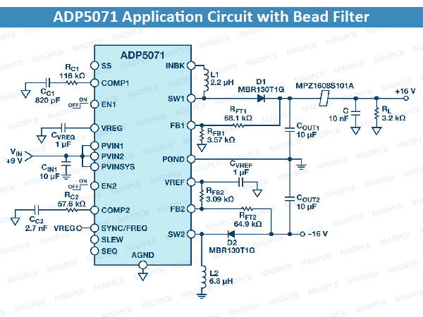
ADP5071 Application Circuit with Bead Filter
As an example, Figure above shows an ADP5071 application circuit with an implemented bead filter and Figure below shows the spectral plot at the positive output. The switching frequency is set at 2.4 MHz, the input voltage is 9 V, the output voltage is set at 16 V, and the load current of 5 mA.
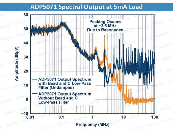
ADP5071 Spectral Output at 5mA Load
Resonant peaking occurs at around 2.5 MHz due to the inductance of the bead and the 10 nF ceramic capacitor. Instead of attenuating the fundamental ripple frequency at 2.4 MHz, a gain of 10 dB occurs.
Other factors that have an effect on the resonant peaks are the series and load impedances of the ferrite bead filter. Peaking is significantly reduced and damped for higher source resistance. However, the load regulation degrades with this approach, making it unrealistic in practice. The output voltage droops with load current due to the drop from the series resistance. Load impedance also affects the peaking response. Peaking is worse for light load conditions.
Damping Methods
This section describes three damping methods that a system engineer can use to reduce the level of resonant peaking significantly. See following figure.
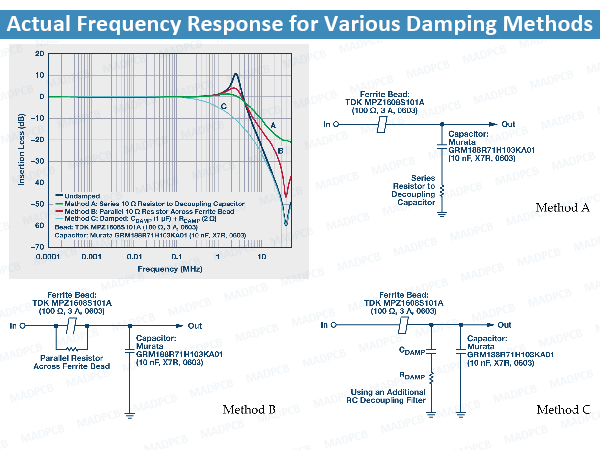
Actual Frequency Response for Various Damping Methods
Method A consists of adding a series resistor to the decoupling capacitor path that dampens the resonance of the system but degrades the bypass effectiveness at high frequencies. Method B consists of adding a small parallel resistor across the ferrite bead that also dampens the resonance of the system. However, the attenuation characteristic of the filter is reduced at high frequencies.
The 2 figures below show the impedance vs. frequency curve of the MPZ1608S101A with and without a 10 Ω parallel resistor. The light green dashed curve is the overall impedance of the bead with a 10 Ω resistor in parallel. The impedance of the bead and resistor combination is significantly reduced and is dominated by the 10 Ω resistor.
However, the 3.8 MHz crossover frequency for the bead with the 10 Ω parallel resistor is much lower than the crossover frequency of the bead on its own at 40.3 MHz. The bead appears resistive at a much lower frequency range, lowering the Q for improved damped performance.
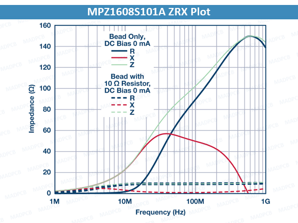
MPZ1608S101A ZRX Plot
MPZ1608S101A ZRX Plot
Method C consists of adding a large capacitor (CDAMP) with a series damping resistor (RDAMP), which is often an optimal solution.
Adding the capacitor and resistor damps the resonance of the system and does not degrade the bypass effectiveness at high frequencies. Implementing this method avoids excessive power dissipation on the resistor due to a large DC blocking capacitor. The capacitor must be much larger than the sum of all decoupling capacitors, which reduces the required damping resistor value. The capacitor impedance must be sufficiently smaller than the damping resistance at the resonant frequency to reduce the peaking.
Figure below shows the ADP5071 positive output spectral plot with Method C damping implemented on the application circuit. The CDAMP and RDAMP used are a 1 µF ceramic capacitor and a 2 Ω SMD resistor, respectively. The fundamental ripple at 2.4 MHz is reduced by 5 dB as opposed to the 10 dB gain.
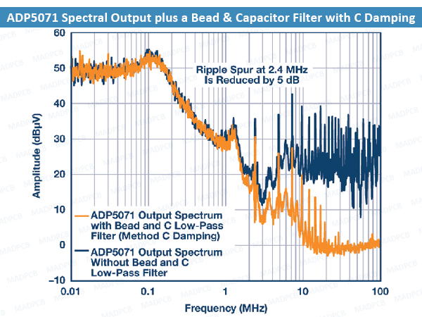
ADP5071 Spectral Output plus a Bead & Capacitor Filter with C Damping
Generally, Method C is the most elegant and is implemented by adding a resistor in series with a ceramic capacitor rather than buying an expensive dedicated damping capacitor. The safest designs always include a resistor that can be tweaked during prototyping and that can be eliminated if not necessary. The only drawbacks are the additional component cost and greater required board space.
Conclusion
This article shows key considerations that must be taken into account when using ferrite beads. It also details a simple circuit model representing the bead. The simulation results show good correlation with the actual measured impedance vs. the frequency response at zero DC bias current.
This article also discusses the effect of the DC bias current on the ferrite bead characteristics. It shows that a DC bias current greater than 20% of the rated current can cause a significant drop in the bead inductance. Such a current can also reduce the effective impedance of the bead and degrade its EMI filtering capability. When using ferrite beads in supply rail with DC bias current, ensure that the current does not cause saturation of the ferrite material and produce significant change of inductance.
Because the ferrite bead is inductive, do not use it with high Q decoupling capacitors without careful attention. Doing so can do more harm than good by producing unwanted resonance in a circuit. However, the damping methods proposed in this article offer an easy solution by using a large decoupling capacitor in series with a damping resistor across the load, thus avoiding unwanted resonance. Applying ferrite beads correctly can be an effective and inexpensive way to reduce high-frequency noise and switching transients.