What’s Forward Bias in PN Junction Diodes?
Forward Bias, or Forward Biasing, is applying potential difference across a p-n diode with a standard polarity, where the anode is connected to the p-region and the cathode is connected to the n-region, that allows current to flow through the junction from p-region to n-region in positive direction. Forward bias decreases the resistance of the depletion layer. A diode (PN junction) in an electrical circuit allows current to flow more easily in one direction than another. Also see Reverse Bias.
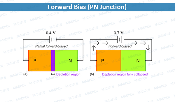
Forward Bias (PN Junction)
When the voltage is applied in the opposite direction across the diode, the depletion region begins to shrink. Here, the applied voltage is opposite to the junction barrier potential. Due to this, effective potential barrier and junction width decrease which further results in more majority of carriers flowing across the junction. Moreover, the amount of voltage required is also less for the complete elimination of the barrier. Forward biased PN junction forces the majority charge carriers to move across the junction. Due to this reason, there is a decrease in the width of the depletion layer.
- The number of holes and electrons are combined with each other once the junction is crossed.
- Each hole in P side combines with an electron that is from the N side. Due to this reason, a covalent bond will break and an electron generated from the covalent bond move towards the positive terminal.
- There is a formation of electron-hole pair.
- Holes carry current in the P region.
- Electrons carry current in the N region.
P-N Junction Diode
A P-N junction diode is a two-electrode semiconductor where the electric current flows only in one direction. The device does not allow the electric current to flow in the opposite direction. If a P-N junction diode facilitates the flow of electric current when the applied voltage is present it is a forward bias P-N junction diode.
Different types of semiconductor materials such as silicon, gallium arsenide, and germanium are used to construct P-N junction diode.
Properties of P-N Junction in Forward Bias
- When any type of P-N junction is in forward bias, a resistor Rs must be connected in series with the diode.
- The function of the limiting resistance is to limit the forward current into the diode.
- When a P-N junction is forward biased the majority carrier of the P and N region will be moving toward the junction and this will reduce the region of immobile charges and therefore the width of the depletion layer is reduced.
- Under forward bias, the field because of the space charge region and forward voltage Vd will be opposing each other. Hence, the resultant electric field is very small and it is experimentally found that the field is always directed from N to P
- When P-N junction is forward bias, the barrier height reduces by |V0| (magnitude of VD)
Diode Operation
The way that a diode operates can be difficult to understand as it involves fairly advanced quantum mechanics. However, at the simplest level the operation of a diode can be understood by looking at the flow of positive charges (or “holes”) and the negative charges (the electrons). Technically, a semiconductor diode is referred to as a p-n junction. These p-n junctions are important in the operation of a photovoltaic cell as well. Having the diode work properly requires a process known as doping. Semiconductors can be doped with materials so that they have an excess of easily displaced electrons – generally referred to as a negative or n-type region. As well, they can be doped with elements that create an excess of holes that easily absorb these electrons – generally referred to as a positive or p-type region. The negative and positive regions of the diode are also the component’s cathode and anode respectively.
The differences between two materials and their interactions over very short distances (less than 1mm) result in a diode when the two types are joined. Joining these two types creates the p-n junction, and the region between the two sides is called the depletion region, as electrons from the n-type region diffuse and fill some of the holes in the p-type region. This creates negative ions the p-type region and leaves behind positive ions in the n-type region. This responds to electric fields difficultly depending on the direction of the electric field. This leads to useful electronic behavior depending on which way the voltage (or electric field) is applied, this is called biasing.
Different Cases
Case 1: If VD< V0 is applied.
Barrier voltage (V0) is dominating. Hence no majority carrier will be crossing the junction. Hence, the forward current is Zero (practically forward current is 10-12 to 10-15A), the diode is now forward biased and non-conducting i.e., it is in OFF state.
Case 2: If VD =V0 is applied
The effect of the barrier is nullified i.e., the barrier hereafter will not oppose any majority carriers in crossing the junction. Both the majority and minority carriers will be crossing the junction. Hence, forward current is small or fwd. current just passes into the diode.
Case 3: If VD > V0
Since the forward voltage of the diode, VD is greater than V0, more majority carrier will be crossing the junction and the forward current exponentially increases with the forward voltage VD. The diode is in conducting state or we can say the diode is in ON state.
Important Consideration for solving numerical
If Ge or Si is not specified in the question, take n = 1
- Is: Reverse saturation current and it is in the range of 10-10 to 10-15 A.
- Is is highly sensitive to temperature.
- Is doubles for every 5oC rise in temperature, but we always apply the thumb rule that this current Is also doubles for 10oC rise in temperature.
- The forward current exponentially increases with the forward voltage across the diode (If = IseV0/nVt)
- When PN junction is forward biased, holes are injected from P to N and e– are injected from N to P.
- This majority carriers of p and n regions are entering a carrier or excess minority carrier.
- Forward current is injected minority carrier current or excess minority carrier current.
In a forward bias p-n junction, the sequence of the events are as follows:
- Injection
- Diffusion
- Recombination
- Forward current is a diffusion current because this current is passing through the junction from higher concentration to lower concentration.
- Forward current flows from p-n and is in mA
- In a forward-biased p-n junction, the current up to the edge of the depletion layer is due to drift of majority carrier.
Considering a p+n junction operating under forward bias, the minority carrier concentration distribution is as follows.
As the minority carrier of p and n regions cross into the opposite regions, they become injected minority carriers. The injected minority carrier concentration will be maximum at the edge of the depletion layer on the opposite side and then they diffuse into the region. Hence, forward current is diffusion current and also it is a minority carrier current.
Forward Current Equation of PN Junction Diode
The diode equation is given as
ID = IS(eqVD/NkT – 1)
Here,
ID = diode current in amps
IS = Saturation current in amps (1 x 10-12 amps)
e = Euler’s constant (∼ 2.718281828)
q = charge of electron (1.6 x 10⁻¹⁹ coulombs)
VD = Voltage applied across diode in volts
N = emission coefficient (between 1 and 2)
k = Boltzmann, s constant (1.38 x 10⁻²³)
T = Junction Temperature
The term kT/q is the voltage produced within the PN junction due to the temperature and this temperature is called the thermal voltage. The value of kT/q is equal to 26 millivolts at room temperature. Let us assume N to be equal to 1. Then the diode equation can be written as
ID = IS(eVD/0.026 – 1)
Please be sure to have your PCB designers and PCB assembly teams working together towards implementing the use of forward and reverse biasing techniques in all of your PCB designs.