What’s Reverse Bias in PN Junction Diodes?
Reverse Bias, or Reverse Biasing, is applying potential difference across a p-n diode with a reverse polarity, where the anode is connected to the n-region and the cathode is connected to the p-region. The negative potential at the p-region attracts the holes and the positive potential at the n-region attracts the free electrons.
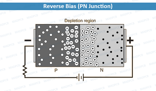
Reverse Bias (PN Junction)
As a result, the depletion region widens and the barrier potential increases. This has the effect of increasing or decreasing the effective resistance of the junction itself allowing or blocking the flow of current through the diodes PN junction. There will not be any current flow due to majority charge carriers. However, a small current flows through the circuit due to minority carriers. Also see Forward Bias.
A diode (PN junction) in an electrical circuit allows current to flow more easily in one direction than another. The voltage with reverse biasing doesn’t cause any appreciable current to flow. This is useful for changing AC current to DC current. It has other uses in manipulating electronic signals as well.
If a voltage is applied across the diode in such a way that the n-type half of the diode was connected to the positive terminal of the voltage source and the p-type half was connected to the negative terminal, electrons from the external circuit would create more negative ions in the p-type region by “filling the holes” and more positive ions would be created in the n-type region as electrons are displaced toward the positive terminal of the voltage source. Hence, the depletion region would increase and the voltage between the p-type and n-type regions would also increase as the total charge on each side of the junction increases in magnitude until the voltage across the diode equals and opposes the applied voltage and cancels it out, ceasing the current through the circuit. This process happens nearly instantaneously and results in essentially no current flow through the circuit when voltage is applied in this direction across the diode. This is known as a reverse-biased p-n junction.
Diode Operation
The way that a diode operates can be difficult to understand as it involves fairly advanced quantum mechanics. However, at the simplest level the operation of a diode can be understood by looking at the flow of positive charges (or “holes”) and the negative charges (the electrons). Technically, a semiconductor diode is referred to as a p-n junction. These p-n junctions are important in the operation of a photovoltaic cell as well. Having the diode work properly requires a process known as doping. Semiconductors can be doped with materials so that they have an excess of easily displaced electrons – generally referred to as a negative or n-type region. As well, they can be doped with elements that create an excess of holes that easily absorb these electrons – generally referred to as a positive or p-type region. The negative and positive regions of the diode are also the component’s cathode and anode respectively.
The differences between two materials and their interactions over very short distances (less than 1mm) result in a diode when the two types are joined. Joining these two types creates the p-n junction, and the region between the two sides is called the depletion region, as electrons from the n-type region diffuse and fill some of the holes in the p-type region. This creates negative ions the p-type region and leaves behind positive ions in the n-type region. This responds to electric fields difficultly depending on the direction of the electric field. This leads to useful electronic behavior depending on which way the voltage (or electric field) is applied, this is called biasing.
Please be sure to have your PCB designers and PCB assembly teams working together towards implementing the use of forward and reverse biasing techniques in all of your PCB designs.