High Density Interconnect (HDI) technology is a printed circuit board that has a higher wiring density per unit area than a conventional PCB. This is achieved using fine line features and clearances, microvias, blind and buried vias and sequential lamination technologies. This name is also used as an alternative to Sequential layer Build-Up (SBU).
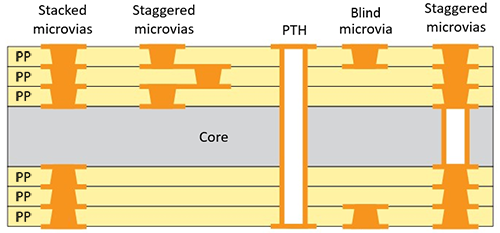
Mircovia Types in HDI PCB Layout
When Considering High Density Interconnect (HDI)?
HDI PCB design is popular, the manufacture gets mature with latest equipment and technologies. Ball Grid Arrays (BGA), the dominant package for complex electronic components, feature sub-millimeter pitch driven forth by the consumer segment and their continual need for integration and miniaturization. Feature sizes demanded by high reliability electronic boards (IPC-6011, class 3) precludes use of packages with pitch smaller than 0.8mm using conventional PCB fabrication process, while popular components are offered with pitch of 0.65mm, 0.4mm and even less. Achieving class 3 compliance when using these packages is only possible by extending the conventional fabrication process with feature collective known as High Density Interconnect (HDI).
HDI Increases Cost but Also Reduces Cost
In low-volume segment, microvias were often added to a lay-up when routing a design using a conventional structure proved difficult or impossible. Adding microvias to a given lay up adds PCB manufacturing cost, so micrivas are often regarded as a cost driver to be avoided if possible. However, designers in the consumer segment use HDI and microvias aggressively to achieve cost down.
HDI’s cost saving potential stems from its efficient use of space and area which in turn results in higher routing density. The via structure itself has smaller diameter and consumes less space. The primary advantage, however, comes from the small vertical extension of the microvia, which leaves larger routing channels on other layers. Judiciously employed it allows a reduction of the number of layers in the board for a given circuit, which more than offsets the cost added by the inclusion of microvias.
Signa Integrity and Power Integrity with HDI Microvias
Microvias in HDI board are also used effectively in improving signal integrity and power integrity. Though-hole vias represent small capacitive loads and stubs which may cause a degradation of high-speed signals. Smaller, shorter microvias presents reduced parasitic loads and allows for routing without via stubs. Filled and capped microvias placed directly in component solder lands reduces inductance in the power distribution network. Microvia in pad is advantageous for high speed signaling as well.
Larger processor chips may pull several tens of Ampere and experience significant load steps. The grid of large through-hole vias under dense BGAs often perforate the power and ground planes that supply this current to an extent where the flow is restricted. Microvias, with smaller diameter and limited depth, reduces the perforation and helps limit ripple and voltage drops to an acceptable level.
HDI Microvias Reduces Board Layers
The escape routing from larger BGAs usually determines the number of routing layers required in a complex PCB. Most connections must be channeled directly to an inner layer to be routed out of the BGA area. With a conventional PCB structure, the result is a dense grid of through-hole vias that obstruct the path for nets to escape. With 1mm pitch, only a single trace may pass between two adjacent vias resulting in a massive growth in the layer count as the array grows. HDI allows for smaller track and space, and with fewer vias extending through the board, broader routing channels may be established. The result is a higher routing density and significant reduction of the number of routing layers required.
Using Staggered or Stacked Microvias in Your HDI PCB?
When a signal must travels several levels of microvias, vias on subsequential layers may be placed with a small offset, in a staggered fashion. It is, however, also possible to stack them right on top of each other and also on top of buried vias. Stacking microvias is more space efficient and makes for easier routing, but there is a cost in terms of reliability.
A single microvia by itself is the most reliable interconnect structure of all with staggered microvias as a close second. Stacked vias will experience greater thermal stress during the reflow soldering process and is generally less reliable than a conventional through-hole via. The buried via is considered the least reliable structure depending on the details of its formation. For high-reliability HDI boards, it is advisable to use staggered structure, and to take great care in specifying the buried vias.
Much Care and Knowledge in HDI Board Manufacturing
Adding high density interconnect (HDI) features to your PCB design only after a designer has struggled and failed to route if using conventional structure adds cost without benefit. No one will make good design decisions in desperation and on overtime. It is smarter to assess if a complex design could benefit from HDI and consider the various design options up front.
Realizing the full advantage of HDI technology takes careful planning and in-depth knowledge of construction techniques, processes and materials in HDI Board manufacturing. And close cooperation with a capable PCB fabricator from the outset is mandatory.