What is an IGFET?
An IGFET (Insulated Gate Field-effect Transistor) is a unipolar device, just like JFET: that is, the controlled current does not have to cross a PN junction. There is a PN junction inside the transistor, but its only purpose is to provide that nonconducting depletion region which is used to restrict current through the channel. IGFET is sometimes referred to as a MOSFET.
There is more than one type of field-effect transistor (FET).
- Junction field-effect transistor (JFET) uses voltage applied across a reverse-biased PN junction to control the width of that junction’s depletion region, which then controls the conductivity of a semiconductor channel through which the controlled current moves.
- Insulated Gate Field-Effect Transistor (IGFET) exploits a similar principle of a primarily from the JFET in that there is no direct connection between the gate lead and the semiconductor material itself. Rather, the gate lead is insulated from the transistor body by a thin barrier, hence the term insulated gate. This insulating barrier acts as the dielectric layer of a capacitor and allows gate-to-source voltage to influence the depletion region electrostatically rather than by direct connection.
In addition to a choice of N-channel versus P-channel design, IGFETs come in two major types: enhancement and deletion. The depletion type is more closely related to the JFET, so we will begin our study of IGFETs with it.
Schematic Symbol and Physical Diagram
Here is a diagram of an N-channel IGFET of the “depletion” type:
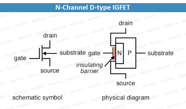
N-Channel D-type IGFET
Notice how the source and drain leads connect to either end of the N channel, and how the gate lead attaches to a metal plate separated from the channel by a thin insulating barrier. That barrier is sometimes made from silicon dioxide (the primary chemical compound found in sand), which is a very good insulator. Due to this Metal (gate) – Oxide (barrier) – Semiconductor (channel) construction, the IGFET is sometimes referred to as a MOSFET. There are other types of IGFET construction, though, and so “IGFET” is the better descriptor for this general class of transistors.
Notice also how there are four connections to the IGFET. In practice, the substrate lead is directly connected to the source lead to make the two electrically common. Usually, this connection is made internally to the IGFET, eliminating the separate substrate connection, resulting in a three-terminal device with a slightly different schematic symbol:
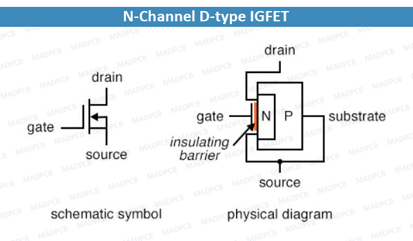
N-Channel D-type IGFET
With the source and substrate common to each other, the N and P layers of the IGFET end up being directly connected to each other through the outside wire. This connection prevents any voltage from being impressed across the PN junction. As a result, a depletion region exists between the two materials, but it can never be expanded or collapsed. JFET operation is based on the expansion of the PN junction’s depletion region, but here in the IGFET that cannot happen, so IGFET operation must be based on a different effect.
Indeed, it is for when a controlling voltage is applied between gate and source, the conductivity of the channel is changed as a result of the depletion region moving closer to or further away from the gate. In other words, the channel’s effective width changes just as with the JFET, but this change in channel width is due to depletion region displacement rather than depletion region expansion.
N-channel IGFET
In an N-channel IGFET, a controlling voltage applied positive (+) to the gate and negative (-) to the source has the effect of repelling the PN junction’s depletion region, expanding the N-type channel and increasing conductivity:
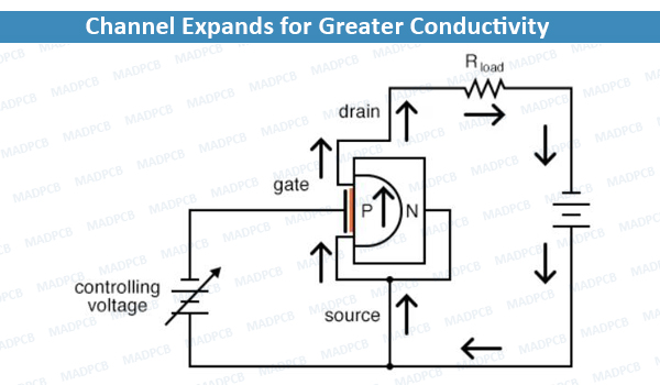
Channel Expands for Greater Conductivity
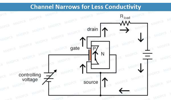
N-channel IGFET
In an N-channel IGFET, a controlling voltage applied positive (+) to the gate and negative (-) to the source has the effect of repelling the PN junction’s depletion region, expanding the N-type channel and increasing conductivity:
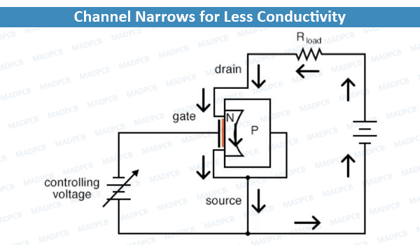
Channel Narrows for Less Conductivity
The insulated gate allows for controlling voltages of any polarity without danger of forward-biasing a junction, as was the concern with JFETs. This type of IGFET, although it’s called a “depletion-type,” actually has the capability of having its channel either depleted (channel narrowed) or enhanced (channel expanded). Input voltage polarity determines which way the channel will be influenced.
Understanding which polarity has which effect is not as difficult as it may seem. The key is to consider the type of semiconductor doping used in the channel (N-channel or P-channel?), then relate that doping type to the side of the input voltage source connected to the channel by means of the source lead. If the IGFET is an N-channel and the input voltage is connected so that the positive (+) side is on the gate while the negative (-) side is on the source, the channel will be enhanced as extra electrons build up on the channel side of the dielectric barrier. Think, “negative (-) correlates with N-type, thus enhancing the channel with the right type of charge carrier (electrons) and making it more conductive.” Conversely, if the input voltage is connected to an N-channel IGFET the other way, so that negative (-) connects to the gate while positive (+) connects to the source, free electrons will be “robbed” from the channel as the gate-channel capacitor charges, thus depleting the channel of majority charge carriers and making it less conductive.
P-channel IGFET
For P-channel IGFETs, the input voltage polarity and channel effects follow the same rule. That is to say, it takes just the opposite polarity as an N-channel IGFET to either deplete or enhance:
Channel Expands for Greater Conductivity
Channel Narrows for Less Conductivity
Illustrating the proper biasing polarities with standard IGFET symbols:
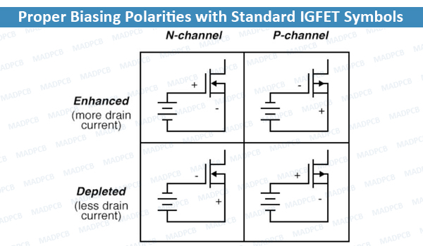
Proper Biasing Polarities with Standard IGFET Symbols
When there is zero voltage applied between gate and source, the IGFET will conduct current between source and drain, but not as much current as it would if it were enhanced by the proper gate voltage. This places the depletion-type, or simply D-type, IGFET in a category of its own in the transistor world. Bipolar junction transistors are normally-off devices: with no base current, they block any current from going through the collector. Junction field-effect transistors are normally-on devices: with zero applied gate-to-source voltage, they allow maximum drain current (actually, you can coax a JFET into greater drain currents by applying a very small forward-bias voltage between gate and source, but this should never be done in practice for risk of damaging its fragile PN junction). D-type IGFETs, however, are normally half-on devices: with no gate-to-source voltage, their conduction level is somewhere between cutoff and full saturation. Also, they will tolerate applied gate-source voltages of any polarity, the PN junction being immune from damage due to the insulating barrier and especially the direct connection between source and substrate preventing any voltage differential across the junction.
Ironically, the conduction behavior of a D-type IGFET is strikingly similar to that of an electron tube of the triode/tetrode/pentode variety. These devices were voltage-controlled current regulators that likewise allowed current through them with zero controlling voltage applied. A controlling voltage of one polarity (grid negative and cathode positive) would diminish conductivity through the tube while a voltage of the other polarity (grid positive and cathode negative) would enhance conductivity. I find it curious that one of the later transistor designs invented exhibits the same basic properties of the very first active (electronic) device.