What’s LLP Package?
The Leadless Leadframe Package (LLP) is a leadframe based chip scale package (CSP) that may enhance chip speed, reduce thermal impedance, and reduce the printed circuit board (PCB) space required for SMT assembly. The small size and very low profile make this package ideal for high density PCBs used in small-scale electronic applications, such as cellular phones, pagers, and handheld PDAs. The LLP package is offered in the Pullback and no Pullback configuration. In the Pullback configuration the standard solder pads extend and terminate at the edge of the package. This feature offers a visible solder fillet after circuit board mounting.
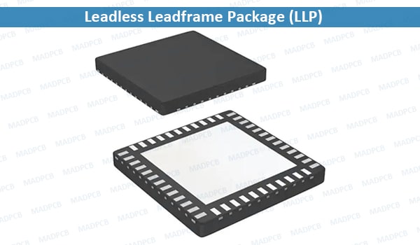
Leadless Leadframe Package (LLP)
The LLP has the following advantages:
- Low profile resistance
- Reduced electrical parasitics
- Improved board space efficiency
- Reduced package height
- Reduced package mass
JEDEC Registration Information:
- Quad LLP Packages: MO-220
- Dual-in-line Packages: MO-229
Terminal Contacts
- The contact pads (or solder pad) are located peripherally in single row format depending on the specific number of pins and body size.
- For certain specific applications, the packages are incorporated with common power and/or ground pins.
- All LLP contacts are plated with 85Sn/15Pb solder for ease of surface mount processing.
- All Lead-Free LLP contacts are plated with matte tin solder for ease of surface mount processing.
Printed Circuit Board (PCB) Footprint
- Soldering the exposed die attach pad (DAP) to the PCB provides 3 advantages, including optimizing thermal performance, enhancing solder joint reliability, and facilitating package self-alignment to the PCB during reflow soldering.
- The LLP is offered in either dual-in-line (DIP) or quad configuration, and Pullback or No Pullback terminal contact designs.
- The LLP package also comes in different thickness. 0.8mm is the most prevalent thickness but the package is selectively available also in 0.6mm and 0.4mm thickness. The terminal pitch ranges from 0.4mm to 1.0mm.
- Coplanarity is not an area of concern for this package. All contacts are flush with the bottom of the package.
- Moisture Sensitivity Level (MSL) of specific applications, requiring large packages, may vary depending on die size, exposed DAP design, and number of downbonds.
- The package with solder bumps is also offered in the Pullback option only. The bump LLP does not require a solder printing process during surface mounting. It can be mounted by flux dipping / dispensing to the PCB board and reflow. The solder bump on the package will melt and form the solder joint between the package and circuit board.