What’s micro SMD?
Micro SMD is a wafer level chip-scale package (WLCSP), was first introduced by National Instrument in September 1998. Micro SMD package has the following features:
- Package size equal to die size
- Smallest footprint per I/O count
- No need for underfill material
- Interconnect layout available in 0.4mm or 0.5mm pitch
- No interposer between the silicon IC and the printed circuit board (PCB)
- Both lead-free and Sn/Pb Eutectic solder versions available
Package Construction
The figure below shows the typical microSMD products. They have solder bumps located on the device side of silicon IC. The micro SMD manufacturing process steps include standard wafer fabrication process, wafer re-passivation, deposition of solder bumps on I/O pads, application of protective encapsulation coating, testing using wafer sort platform, laser marking, singulation and packing in tape and reel. The package is assembled on PCB using standard surface mount techniques (SMT).
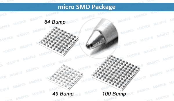
micro SMD Package
Micro SMD Package Data
|
Package Arrays |
|
| Bump Count |
Array Outline |
|
36 |
6 x 6 |
| 42 |
6 x 7 |
|
49 |
7 x 7 |
| 56 |
7 x 8 |
|
64 |
8 x 8 |
| 80 |
8 x 10 |
|
81 |
9 x 9 |
| 100 |
10 x 10 |
|
Bump Size Details |
||
| Bump Diameter (mm) |
0.32 |
0.265 |
| Pitch (mm) |
0.5 |
0.4 |
| Bump Count Range |
36-100 |
|
| Package Thickness Nominal (mm) |
0.65 |
|
| Bump Height Nominal (mm) |
0.255 |
0.21 |
| Bump Coplanarity within Package (mm) |
0.015 |
|
| Shipping Media |
Tape & Reel |
|
| Moisture Sensitivity Level |
Level 1 |
|
Surface Mount Assembly Considerations
Its surface mount assembly operations includes,
- Printing solder paste on PCB
- Component placement using standard pick and place equipment
- Solder reflow and cleaning (depending on flux type)
Advantages of microSMD during SMT assembly includes,
- Standard tape and reel shipping media eases handling issues (per EIA-481-1)
- Uses standard SMT pick and place equipment
- Standard reflow process (both Lead-free and Sn/Pb eutectic compatible)