What is ODFN Package?
Optical Dual-in-line Flat No-lead (ODFN) packages are developed for light sensor applications. The mechanical structure of an ODFN is similar to that of a conventional DFN, except the molding compound is a transparent material rather than the conventional black compound. Transparent molding compound allows transmission of ambient light through the molding compound to reach the die sensor area. This package is Lead-free, with pre-plated Nickel-Palladium-Gold (NiPdAu) finish on the terminals.
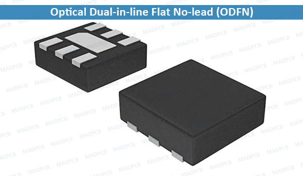
Optical Dual-in-line Flat No-lead (ODFN)
ODFN package follows conventional DFN/QFN guidelines for PCB land pattern design and surface mount processing. Some additional recommendations are made to accommodate the special clear mold compound, which has a lower glass transition temperature (Tg) and a higher coefficient of thermal expansion (CTE) compared to conventional molding compounds.
Board Mounting Guidelines
The package board mounting process is similar to that of conventional DFN/QFN packages. However, there are some key differences in the materials used, therefore it is recommended that users account for these differences in their application method. Specific guidelines in this document are meant to accommodate for the differences in the materials.
Product Packing
ODFN products have been qualified under JEDEC MSL-3 test criteria, and are shipped in either a tube or tape-and-reel format. The packaging quantity varies depending on the application and purchasing options. The moisture protection seal should not be broken until the board mounting process is ready. If the seal is broken, please follow standard instructions for baking per JEDEC standard criteria MSL-3 products.
Package Construction
ODFN packages have a nominal package thickness of 0.7mm. It is important to design PCB land patterns that correspond to the lead dimension as explained in subsequent section. Similar to DFN and QFN packages, the ODFN has an exposed die paddle/pad as part of the package construction, the chamfered corner of the exposed thermal pad indicates Pin 1 location for the product. Similar to DFN or QFN, the exposed pad provides robustness to the overall solder joint strength after PCB surface mount process.
ODFN packages are assembled on plated copper lead-frames, and individual units are singulated by sawing process. The occasional presence of a slight oxide layer at the sawn surface of the copper leads is not a concern for solder joint quality. Poor wetting to this exposed side edge does not impact the solder joint quality or reliability.
Solder Stencil
Either 0.100mm or 0.125mm thick stainless steel stencil is recommended in SMT PCB assembly. The stencil should be laser-cut followed by electro-polish (chemical finishing is not recommended), or alternatively an additive build-up stencil may be used. Higher reliability on board can be obtained by increased solder paste volumes. However, this needs to be controlled as solder bridging may occur when the solder paste is excessive.
It is highly recommended to solder the exposed package pad to the corresponding landing pad on the PCB. At the same time, excessive solder under the exposed area may lead to open solder joints under the functional pins due to excess stand-off created by the central pad. Therefore, it is important to balance openings for the pins and opening for exposed pad area. The optimal value for center pad is considered to be 70% to 80% solder paste coverage under the exposed pad area.
Solder Paste
The package itself is lead-free, and is compatible with both eutectic tin/lead or lead-free tin/silver/copper solders. These packages have been qualified at a +240oC maximum temperature reflow profile for eutectic solder, and at a +260oC maximum temperature reflow profile for lead-free solder. Solder paste with “no-clean” flux and “type 3” or “type 4” solder particle size distribution is recommended.