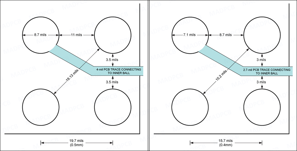
In printed circuit boards, Pitch is the center-to-center distance between two adjacent holes, BGA pads, part connectors, or other SMD pads.
How to Route the Traces with Limited IC Pitch Size?
There is a wide array of ICs that are available in a 0.4mm or 0.5mm pitch. The pitch size refers to the distance between the solder balls on the IC.
- A 0.5mm (19.68mil) pitch gives you approximately 19.7mil of space between solder balls from center-to-center. A typical pad size is 8.7mil, giving you 11mil between pads to route traces. Using a trace-to-solder-ball clearance of 3.5mil, you can comfortably fit a trace width of approximately 4mil between two defined solder ball pads. With a 4mil trace using 1oz copper, you are limited to approximately 220mA current through the trace. With 2oz copper, you can drive 380mA through a 4mil trace.
- A 0.4mm (15.7mil) pitch design can be a bit trickier than a 0.5mm design. There is a lot less space to route traces between solder balls, which means more restriction and less flexibility. A typical pad size is 7mil, leaving you with 8.7mil between pads to route traces. When using a 3mil space on each side of an inner trace, you are only left with a maximum trace width of 2.7mil. With a 2.7mil trace using 1oz copper, you are limited to approximately 160mA current through the trace. For smaller pitch such as 0.4mm, using thicker copper can be a concern, since the trace width is less than the copper thickness (e.g.: 2oz copper = 2.8mil). This can result in a net trace width of less than 2.7mil after the etching and plating process.
- If using a thinner trace between WLP pads does not work for your design, as is such for smaller-pitch WLPs (i.e., 0.3mm), other options can be used. One option is to use a laser microvia, which comes at a premium PCB cost.
We provide a recommendation of trace width to copper thickness from a common PCB fab house.
|
Copper Width |
Copper Thickness | Recommended Trace Width |
| 0.5oz | 0.7mil |
3mil ~ 5mil |
|
1oz |
1.4mil | 4mil ~ 7mil |
| 2oz | 2.8mil |
8mil ~ 10mil |

