What Is A Package on A Package (PoP)?
Package on Package (PoP) is an integrated circuit (IC) packaging method to combine vertically discrete logic and memory ball grid array (BGA) packages. Two or more packages are installed at top each other, i.e. stacked, with a standard interface to route signals between them. This allows higher component density in devices, such as mobile phones, personal digital assistants (PDA), and digital cameras, at the cost of slightly higher height requirements. Stacks with more than 2 packages are uncommon, due to heat dissipation considerations.
A package on package (PoP) typically includes a RAM chip on top and a CPU chip on the bottom. See BGA and chip package.
PoP Configuration
Two widely used configurations exist for PoP:
- Pure memory stacking: two or more memory only packages are stacked on each other
- Mixed logic-memory stacking: logic (CPU) package on the bottom, memory package on top. For example, the bottom could be a system on a chip (SoC) for a mobile phone. The logic package is on the bottom because it needs many more BGA connections to the motherboard.
During PCB assembly, the bottom package of a PoP stack is placed directly on the printed circuit board (PCB), and the other package(s) of the stack are stacked on top. The packages of a PoP stack become attached to each other (and to the PCB) during reflow soldering.
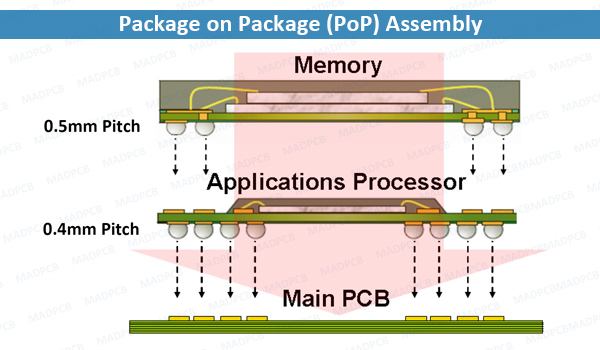
Package on Package (PoP) Assembly
PoP technology allow certain components to be stacked on top of one another during the PCB assembly process; for example, some advanced PoP application processors will have their memory modules mounted directly on top of the main processor package. This technology offers key advantages in miniaturization for many HDI designs, but also requires special consideration during PCB assembly, including multiple placements and/or reflow soldering cycles. These additional considerations can drive up both cost and lead time for a PCB assembly project.
There are two common techniques used for PoP assembly, including one-pass and two-pass. But MADPCB recommends the one-pass PoP assembly, as it is the most economical and produces approximately the same assembly yield. Assembly of PoP devices and PCBs for fine-pitch BGA packages at 0.5mm and smaller is still new for most PCB assemblers. Assembly success comes from experienced companies willing to work together. The most common pairing is an assembly vendor and a PCB fabricator. MADPCB is the company which you want to find, since it is a turnkey PCB and assembly manufacturer, and has Package-on-Package assembly experience, and does not require more time for learning cycles.
Package on Package (PoP) Assembly
- One-Pass: In a one-pass assembly the applications processor is first mounted to the main printed circuit board (PCB), the memory is mounted to the applications processor, and the finished printed circuit board is then run through the reflow oven in a single pass. See the figure above.
- Two-Pass: The two-pass assembly has an intermediate step in which the companion memory is first mounted to the applications processor; then these two parts are placed in a carrier tray and reflowed. These joined devices are then mounted on the main PCB and the finished PCB is reflowed a second time.