What is an Electric Pulse?
An Electric Pulse is a burst of current, voltage, or electromagnetic-filed energy. In practical electronic and computer systems, a pulse may last from a fraction of picosecond up to several seconds or even minutes. In digital systems, pulses comprise brief burst of DC (direct current) voltage, with each burst having an abrupt beginning (or rise) and an abrupt ending (or delay).
In digital circuits, pulses can make the voltage either more positive or more negative. Usually, the more positive voltage is called the high state and the more negative voltage is called the low state. The length of time between the rise and the decay of a single pulse is called the pulse duration or pulse width. Multiple pulses often occur in a sequence called a pulse train, where the length of time from the beginning of one pulse to the beginning of the next is called the pulse interval.
Digital pulses usually have well-defined shapes (voltage-vs.-time graphs, as might be observed on an oscilloscope ) such as rectangular or triangular. In nature, however, pulses can have irregular shapes and can occur at random intervals. A good example is an EMP (electromagnetic pulse) generated by a lightning discharge in a thunderstorm, a solar flare, or a transient “voltage spike” that can occasionally occur on a utility power line.
Pulse Plating in PCB Manufacturing
The continuing trend of miniaturization is driving PCB design more and more towards HDI and multi-layer boards. This means finer tracks, smaller holes and higher aspect ratios. As a consequence, the conventional acid-copper electroplating becomes very demanding and affects the performance and the price of the finished board. The ability to plate sophisticated boards is given by the use of pulse current instead of a DC. Since the pulse plating process takes place at higher current densities, a fine grain structure of the deposit can be obtained and hence the deposit porosity is reduced.
Uniform deposit distribution is another advantage offered by the pulse technology. It should be noted, that current “shaping” represents only one way of influencing the complicated system which contains many other process parameters. To understand the interdependence of these parameters with pulse parameters qualitatively, a basic mass transport and its influence to the current distribution are described. Charging and discharging of the double layer, which is a side effect of the pulse plating, represents the main limitation of arbitrary pulse parameters setting. It can be reduced providing sufficient slopes of current pulses. Considering this, we also proposed a new topology of pulse current source and built an experimental model. At the end, the results of copper deposition obtained under bipolar pulse current conditions are collected and compared to the results obtained using conventional technology.
Laser PCB with Shorter Pulses, Shorter Wavelengths
The electronics industry is characterized by a relentless drive to deliver increased miniaturization and higher functionality. This impacts virtually every level of electronics fabrication, including two critical micromachining steps in the production of both rigid printed circuit boards (PCBs)—including package substrates—and thin flex circuits. Specifically, these are:
- Drilling blind and through holes, like vias and microvias, which are then electroplated to electrically connect the different layers.
- Cutting or trimming individual circuit boards/substrates.
These laser-based processes are reaching the spatial limitations of established laser technology. As such, there is a transitioning towards the use of ultrashort pulse (USP) lasers with short (green and ultraviolet (UV)) wavelengths.
The drilling and cutting of PCBs and flex circuits require that the heat affected zone (HAZ) is minimized, meaning material adjacent to the cut or hole must be thermally degraded in some way. HAZ can be minimized using USP lasers. The use of shorter pulses results in a colder process. This is because the pulse duration is shorter than the thermal diffusion time in organic materials. In other words, much of the pulse energy is taken away in the ejected evaporated material before it has time to spread, as shown in figure below.
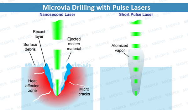
Microvia Drilling with Pulse Lasers
Much of a USP laser’s pulse energy is carried away in the ejected material, resulting in a major reduction in HAZ for virtually all materials.
USP lasers have lower pulse energies than, for example, nanosecond lasers, but process throughput is high because the reduced pulse energy is offset by the lower ablation threshold due to the higher peak power. Moreover, USP lasers are capable of much higher pulse repetition rates and therefore support processing in fast multiple passes, making them well-suited to selective machining of thinner layers on top of substrates that are often ceramic based. For most applications, the total thickness is 1 mm or less, but for specialty applications, such as in the automotive industry, the overall thickness can be up to 2mm.
The key laser-based processes for PCBs are drilling blind vias to form connections between the top conductor layer and targeted lower layers of the circuit board, followed by cutting individual circuit boards/substrates from the larger panel used for high-volume fabrication. The diameters of the vias are currently in the 50–100 μm range, and the final PCBs are typically simple squares or rectangles, so there is no shape complexity except for the occasional cutout. Traditionally, drilling and cutting have both been mechanical processes that rely on the use of saws and drill bits.
A typical drilling machine for via diameters of 100 μm incorporates six drill bits, each capable of producing 20 holes/s, but they only have a lifetime of 2,000 holes. Over the last decade, these machines have been largely replaced by machines that use sealed carbon dioxide (CO2) lasers, such as mid-infrared lasers, which afford exceptional power/cost ratios. However, CO2 lasers are unable to deliver the requisite resolution and produce too much HAZ for via diameters of 50 μm and less. For these applications, green nanosecond lasers have often been preferred, green USP picosecond lasers can achieve the required small diameters and less HAZ at higher speeds. These lasers offer the high pulse repetition rates (5,000 kHz and higher) and high power needed to drill up to 3,000 holes/s if used alongside fast galvanometer scanners.
The UV nanosecond laser is the most commonly used laser for cutting PCBs. However, the longer pulses cause edge discoloration, which impacts perceived value and leaves behind debris, thus necessitating post-process cleaning that does not damage the circuitry. As a result, PCB manufacturers are increasingly looking to green or infrared (IR) USP lasers for a single-step cutting process. IR USP lasers deliver the highest power at the lowest cost, but green USP lasers deliver the best results.
Picosecond Laser Application in Flex circuits
Flex circuits are laminates of copper and a flexible polymer, such as polyimide (PI), and, less commonly, copper (FCCL) and liquid crystal polymer (LCP). To deliver the requisite flexibility, they are much thinner than rigid PCBs, affording typical thicknesses in the 100–300 µm range.
The key laser processes for flex circuits are again drilling and cutting. For several years, these tasks have been mainly the domain of nanosecond UV lasers with a wavelength of 355 nm. However, a growing number of PCB manufacturers are looking to picosecond UV lasers to cut the narrow features and complex curved/shaped contours that flex circuit applications increasingly require. Nanosecond UV lasers are limited to a repetition rate of a few hundred kHz, but picosecond lasers can reach 1000s of kHz. This, as well as the aforementioned lower ablation threshold, means that picosecond UV lasers can deliver a cutting speed up to 10 times higher than that of nanosecond UV lasers. Specifically, it has been demonstrated that if one of these lasers is operated at 50 W with a repetition of 5 MHz, effective cutting speeds up to 1,300 mm/s are achievable for polyimide flex circuits up to 130 µm in thickness with a cutting width of less than 30 µm and a HAZ of less than 10 µm.
Low HAZ is also attributable to another feature of picosecond UV lasers. As the beam scans complex patterns, speed inevitably changes for straight and curved cuts and switches in motion directions. Fixed pulse rates mean excessive dwell time and increased HAZ at cut corners. However, picosecond UV laser allows the laser pulse rate to be slaved to the scanners and the pulse energy to be kept constant, irrespective of the scan speed. This guarantees the same high cut quality in the corners of cutting contours.
Picosecond UV lasers deliver noticeably better hole quality than nanosecond lasers, as shown in figure 5. Furthermore, flex circuit manufacturers are looking to use a single machine to perform both drilling and cutting, and these USP lasers are poised for success in both tasks.
Blind via holes in a flex circuit. The diameter and depth of the holes were 50 µm and 30 µm, respectively. They were drilled in 30 µm thick ABF on copper picosecond UV laser operated at 10 W with a repetition rate of 1 MHz. The drill rate was >3,000 holes/s. The holes show almost no taper. The center image is the top of the holes and the right image is the bottom of the holes.
Drilling and cutting tasks in PCB and flex circuit manufacture are pushing the limits of longer pulsed laser methods. Fortunately, the latest USP lasers deliver both the higher speeds and improved results that these applications now demand.