What is Reactance in PCB?
Reactance, also known as Electrical Reactance, is defined as the opposition to the flow of current from a circuit element due to its inductance and capacitance. An ideal resistor has zero reactance, whereas ideal inductors and capacitors have zero resistance. As frequency increases, inductive reactance increases and capacitive reactance decreases.
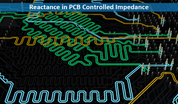
Reactance in PCB Controlled Impedance
Controlled Impedance: Sum of Capacitance & Inductance
Impedance is the combination of the capacitance and inductance of a circuit when operated at high frequency. Though also measured in Ohms, it is somewhat different than resistance which is a DC characteristic. Impedance is an AC characteristic, meaning that it is related to frequency, resistance is not.
The reactance is the opposition to current flow resulting from the effect of the inherent capacitance and of the PCB copper conductor interacting with changes in voltage and current. In DC circuits, there is no reactance and the resistance of copper conductors is typically insignificant.
However, in high-speed AC circuits (those with sharp changes in voltage and/or current), the capacitance and inductance, and thus the impedance can become very significant. This can become critical t a PCB design’s functionality because of the effects that changes in the impedance along the signals path from transmitter to receiver will have on the efficiency of power transfer as well as signal integrity. While a circuit’s speed is often expressed as the frequency of the wave form: the critical concern is the speed at which the voltage and/or current is required to change.
What Determines Controlled Impedance in PCB?
The characteristic impedance of a PCB trace is typically determined by its inductive and capacitive reactance, resistance, and conductance. Theses factors are a function of the physical dimensions of the trace, the dielectric constant (Dk) of the PCB substrate material, and dielectric thickness. Typically, PCB trace impedance can range from 25 to 125Ohms. The impedance value generated from the PCB structure will be determined by the following factors:
- Width and thickness of the copper signal trace (top and bottom)
- Thickness of the core or prepreg material on either side of the copper trace
- Dielectric constant of the core and prepreg (PP) material
- Distance from other copper features
Signals will follow the path of least reactance back to the ground return when travelling in the ground plane. In PCB design, the path of least reactance in a star, point-to-point, or multipoint topology should lie directly beneath conductors in your printed circuit board (PCB). This will ensure your circuits have minimized loop inductance after PCB manufacturing and assembly and will have least susceptibility to EMI.