What Is Sheet Resistance in PCB?
In printed circuit board (PCB), Sheet Resistance, also called Sheet Resistivity, or Surface Resistivity is an important property to quantity the ability for charge to travel along the uniform thin films, like carbon, copper, silver inks and pastes, formed by screen or inkjet printing technology.
Sheet Resistance Applications in Printed Electronics
Carbon, silver and copper inks and pastes are usually used for printing patterns to fabricate printed electronics. Silver and copper pastes sometimes are used to filling PCB vias to achieve highest thermal conductivity and lowest resistance. There are many applications:
- Smart glass
- Heaters
- Antenna
- Printed circuit boards
- In-Mold electronics
- Sensors
- Solar / Photovoltaic
- Display
- Wearable / Stretchable
How to Measure Sheet Resistance?
The most common technique used for measuring sheet resistance is the Four-Probe Method. This technical involves using four equally-spaced, co-linear probes (knowns as a Four-Point Probe) to make electrical contact with the material. Most four-probes available commercially use sharp needles as probes. These can scratch or pierce delicate materials often used in thin film electronic devices. This can make it difficult to take accurate sheet resistance measurements, and result in the thin film becoming unusable. The below figure shows the Four-Point Probe Device used at MADPCB.
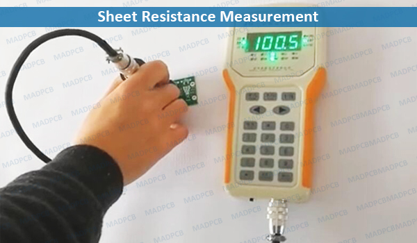
Sheet Resistance Measurement on PCB
This is designed to overcome these issues. This device utilizes spring-loading probes with rounded tips that apply a contact 60 grams of force whilst in contact. Additionally, contact s made using a precision vertical translation stage that is operated with a micrometer to allow for soft, controlled contact with the sample.
What Is the Four-Probe Method?
The four-probe method works by contacting four equally-spaced, co-linear probes to the material. This is known as a four-point probe, and a schematic is shown in following figure.
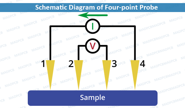
Schematic Diagram of Four-point Probe
A DC current is applied between the outer two probes (number 1 and 4) and a voltage drop is measured between the inner two probes (number 2 and 3). The sheet resistance can then be calculated using the following equation:
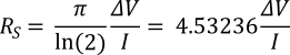
Sheet Resistance Calculation Equation
Where:
RS: sheet resistance
ΔV:the change in voltage measured between the inner probes
I: the current applied between the outer probes
The sheet resistance is expressed with the units Ω/sq, Ω/□, or “ohms per square”, to differentiate it from bulk resistance.
In addition to the factor of π/ln(2), a geometric correction factor is often required. The correction factor is based upon the size and shape of the sample, as well as the positioning of the probes, and accounts for the limitation of current pathways through it. However, it should be noted that the most accurate measurements are taken from the center of the sample.
If the thickness of the measured thin-film material is known, then the sheet resistance can be used to calculate its resistivity:
ρ=RS · t
Where ρ is the resistivity, and t is the thickness of the material.
This technique is also known as the Kelvin technique, a method of eliminating wire and contact resistance from a resistance measurement. Figure following shows the circuit resistance of a four-probe measurement.
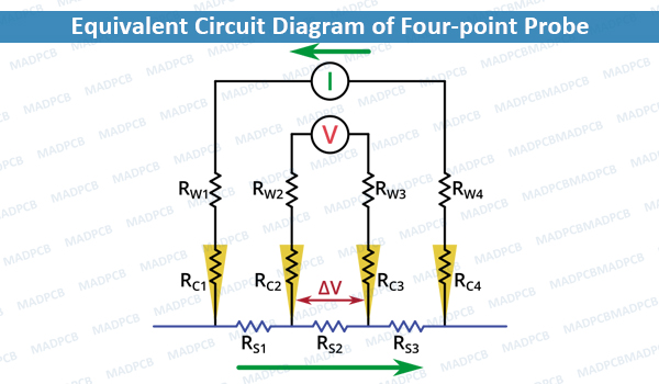
Equivalent Circuit Diagram of Four-point Probe
As no current flows through the inner two probes, the wire resistance of RW2 and RW3 and the contact resistance of RC2 and RC3 do not affect the voltage measured at the voltmeter. This means that the measured decrease in voltage (ΔV) between the inner two probes arises entirely from RS2. Therefore, ΔV can be used along with the applied current in the RS equation to calculate the value of RS2 (i.e. the sheet resistance).