What Is A Solder Paste Layer?
A Solder Paste Layer, or Paste Mask Layer in Gerber files is used to define the exposed copper pad features on bare boards in PCB manufacturing, and is mainly used to customize solder paste stencil in PCB assembly. Thus, a solder paste layer is also called a Stencil File. In single-sided assembly board, there is only one stencil file, either top or bottom; In double-sided assembly board, there are two stencil files -both top and bottom.
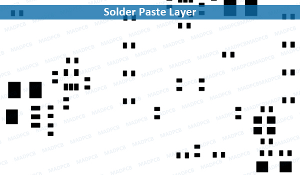
Solder Paste Layer
The copper pad shapes are square, rectangle, round and etc., and their sizes sometimes are the same with SMD pads, or sometimes are slightly smaller. On bare boards, the exposed copper pads are with different surface finishes, some looks gold, some looks tin, and some looks silver, but all of them are for pad anti-oxide protection and for better solderability.
Solder Paste Layer for Customizing SMD Stencil
In a turnkey PCB assembly manufacturer, like MADPCB, both bare board and circuit board assembly will be completed under one roof. When finished the bare boards, an SMT engineer will take a physical circuit board to check the pad properties and compare them with the solder paste layers opened in Gerber viewer, then as per IPC-7525A stencil design guidelines to decide how to customize the windows openings on stencil(s). Generally, he will consider the automated solder paste printer’s working area to decide the stencil’s size; whether need to put the top and bottom solder paste layers on the same stencil; whether make a frameless stencil or a framed stencil upon how large the order quantities.
The Solder Paste Layers are important and sometimes it is separately stored in SMT file folder. Some overseas customers, especially German PCB customers are not willing to forward solder paste layers, silkscreen layers together with other Gerber files to PCB manufacturers. For figure out the copper pads, a CAM engineer has to manual make stencil files in CAM editor as per solder mask layer(s).
No Solder Paste Layers?
Besides, we don’t recommend to make SMT stencils without a physical bare board. After all, the finished pad sizes may be bigger or smaller than Gerber defined sizes, and you cannot compare the stencil windows openings with the exposed pads.