What’s Surface Resistivity in PCB?
Surface Resistivity (ρS) is the measure of the electrical or insulation resistance of the surface of a PCB material. Like volume resistivity, PCB materials are required to have very high values of ρS, in the order of 10⁶Ω/sq – 10¹⁰ MΩ/sq. It is also somewhat affected by both moisture and temperature. Also see Volume Resistivity, Sheet Resistance.
Surface resistivity defines a fixed surface length’s electrical resistance on an insulating material. This measurement does not take physical dimensions, such as thickness and diameter into consideration. Since it only determines the surface’s resistivity, only one physical measurement is required. Accordingly, ρS is measured between electrodes along the insulator material’s surface.
In materials testing, this measurement can determine the ρS of plastics. In situations involving static electricity dissipation such as electronics manufacturing, low surface resistivity is ideal. On their own, engineering plastics have high levels of surface resistance. To increase conductivity, manufacturers often add carbon or a surface treatment. In general, ρS testing is rarely applied to metals because they already have high conductivity.
Surface resistivity describes the local, physical behavior of a PCB surface under a voltage gradient field. The aggregate behavior over all such points creates an equivalent, Parasitic Surface Resistance (RPS) between any two points. Bulk resistivity (ρV, in units of MΩ·cm, or equivalent) describes the local, physical behavior inside a PCB’s dielectric under a voltage gradient field. The aggregate behavior over all such points creates an equivalent, Parasitic Bulk Resistance (RPB) between any two points. Typical resistivities for FR4, based on several manufacturer’s data, are:
- ρS ≈ 1 × 10⁵ MΩ
- ρV ≈ 1 × 10⁶ MΩ·cm
Different operating conditions and manufacturing flows will produce different values; sometimes by two or three orders of magnitude in either direction.
How to Measure Surface Resistivities?
The example below shows two parallel, serpentine traces on the same PCB surface. This geometry is useful for measuring ρS on a given PCB process. Make the traces as long as possible, and as close together as possible, to maximize the surface leakage current. For example, a 6 in × 6 in PCB (60 mils thick) could have two serpentine traces 10 mils wide and 10 mils apart. If the overlap area is 5 in × 5 in, the equivalent length would be 1250 in. With ρS = 1 × 10⁵ MΩ and ρV ≈ 1 × 10⁶ MΩ cm, we estimate RPS ≈ 0.8 MΩ and RPB ≈ 2 GΩ.
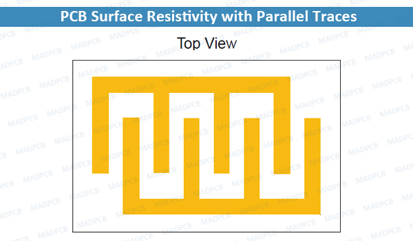
PCB Surface Resistivity with Parallel Traces
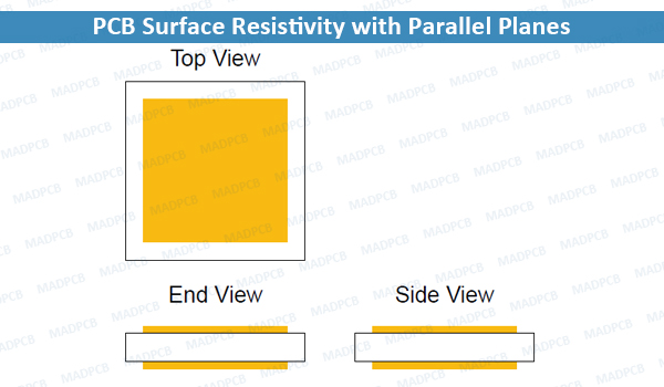
The example below shows two parallel planes on opposite PCB surfaces. This geometry is useful for measuring ρV on a given PCB process. Make the planes as large as possible, to maximize the bulk leakage current. For instance, a 6 in × 6 in PCB (60 mils thick) could have two planes 5 in long and 5 in wide. With ρS = 1 × 10⁵ MΩ and ρV = 1 × 10⁶ MΩ cm, we can estimate RPS ≈ ∞ and RPB ≈ 0.9 GΩ.
Be sure to measure ρS and ρV under various conditions seen by your circuit. These values will also change between different manufacturers and processes.
Numerical Solutions
Software
When optimizing a complicated PCB geometry, it may pay to use a Partial Differential Equation (PDE) solver. Searching the internet for “partial differential equation software,” or the equivalent should bring up several commercially available software packages.
Using Spice
It is possible to use SPICE to implement a network of resistors representing heat flow between adjacent points. Select an array of equally spaced points. Resistors connect adjacent points and represent the local resistance to current flow, in that direction.
To simulate a particular parasitic resistance, force a voltage at its input and measure the current at its output. The voltage-to-current ratio is that resistance.
The figure below shows a typical array point, in a two-dimensional (2D) array. The central point is at voltage V0. The four adjacent points are connected by the four resistors R1, R2, R3, and R4.
The resistors represent the local resistivity between adjacent points. Use very low valued resistors for points connected by metal. For instance, R1 is:
Equation 1:
R1 = ρS Δx / Δy, for surface calculation
R1 = ρV Δx / (Δy Δz), for bulk calculations
Where:
ρS = Local Surface Resistivity (MΩ)
ρV = Local Bulk Resistivity (MΩ cm)
Δx = grid spacing in the x-direction
Δy = grid spacing in the y-direction
Δz = z-dimension (common to all objects)
This approach is easily extended to three dimensions (3D).
Using a Spreadsheet
It is possible to simulate in a spreadsheet by using an iterative approach. Set up the resistive array like the last section. The iteration equation at V0 is:
Equation 2:
V0 = (V1/R1 + V2/R2 + V3/R3 + V4/R4) / (1/R1 + 1/R2 + 1/R3 + 1/R4)
(V1 + V2 + V3 + V4) / 4, all Rs equal
The convergence can be slow, so this approach should be used for simple problems. Once the voltages are determined, it is a simple matter to calculate the sum of currents into (or out of) a node of interest.
This approach is easily extended to three dimensions (3D).