What’s Thieving on PCB?
Thieving is the addition of “dummy” pads (Thieving Pads) across the surface of PCB that are plated along with the features designed onto the outer layers. The purpose of the process is to provide a uniform distribution of copper across the outer copper layers to make plating current and plating in the holes more uniform. These dummy pads are connected together along with all of the other features that will be plated by the outer layer copper laminated onto the PCB stack-up. After plating, the copper between the dummy pads is etched away, leaving them isolated from each other along with other features on the surface layers.
Here is an example of thieving added around components, like around BGA, but which is not common seen in PCB production. In usual applications, these dummy pads are mainly added around press-fit via holes, and on array frames.
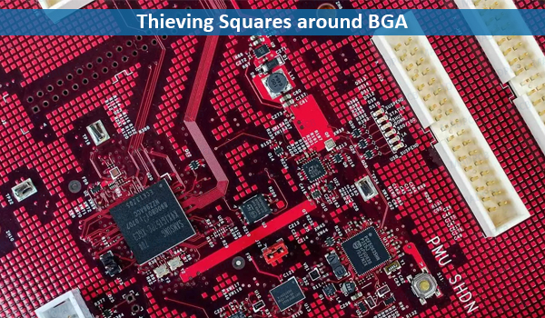
Thieving Squares around BGA
To better understanding thieving, it’s useful to review the plating operations, including outer layer plating, panel plating and pattern plating as described below. Thieving pads can be added in the PCB body or panel frame (/breakaway rail) on outer layers. Thieving is different from the cross hatches on flexible circuit and rigid-flex board. While, thieving is not required on inner layers as they are only exposed to etching and require no plating.
Outer Layer Plating
Outer layer plating is done to deposit copper in the vias and component lead holes so that connections are formed from one side of the PCB to the other. It’s also done to make the connections to signals and planes on inner layers. The two outside layers of a PCB are kept to provide a path for the plating current needed to plate the copper in the holes.
Panel Plating
In the early days of PCB manufacturing, the entire panel on which a PCB was formed would be immersed in the plating bath after the holes had been drilled and the burs and debris were cleaned away. This is referred to as panel plating. The challenge with panel plating is that copper is plated all over the surface even in those area where no traces or pads will be placed after the etching process. This results in two issues:
- The etching of the unwanted copper has to go through the copper plated onto the outer surface as well as the original copper on the outer layer. This requires the use of more chemicals and also takes more time.
- As the etching goes down through the copper it also etches sideways resulting in less accurate trace width control. This led to the pattern plating process described below.
Pattern Plating
Pattern plating is a process where copper is plated up only on those features that will remain behind after the outer layers are finally etched. Usually, the features included are all of the plated through holes, the traces and the component mounting pads. This process is accomplished by applying a plating resist to the two outside layers after drilling has been completed. This plating resist is photosensitive and is exposed to a light that solidifies the resist in areas that are not to be plated. This unexposed resist is washed away, and the areas that must be plated are left exposed. Plating is the next step that takes place.
The problem with pattern plating is that if the features on the outside layers are not evenly distributed across the surface. The plating currents will also not be evenly distributed and some features, such as vias and connector holes, will plate less heavily or uniformly than the others that are spaced farther apart. When there is a need for very uniform plating, such as in the holes of a press-fit connector, something must be done to spread the plating current evenly across the entire surface. This is where thieving comes into play.
How to Add Thieving?
As a printed circuit board manufacturer, MADPCB has algorithms that examine the distribution of copper in the artwork as supplied by the customer. Our CAM engineers will determine how much copper must be added to achieve uniform plating. This extra copper thieving is added in the form of dots or squares. Thieving pads are added by board manufacturers. Different PCB fabricators have their own different shapes (either “dot” or “square”) and sizes for the thieving features.
Thieving May Affect Impedance Control
If there are traces on the layers just below where thieving has been added, the impedance of these traces may be adversely affected if thieving is applied over them. To ensure this does not happen, a note must be added to the fabrication drawing instructing whether thieving is allowed and where it is permitted. The following is one way to specify this on a fabrication drawing:
Thieving is allowed on outer layers to ensure uniform plating. Thieving shall be no closer than 0.100” (2.5 mm) from any other copper feature on the outer layers. It shall not be within 0.100” (2.5 mm) of traces on the first buried signal layer beneath the outer layers. The thieving pattern shall be at the supplier’s discretion and not consist of solid copper.
The Consequences of Not Adding Thieving to Outer Layers
If there are traces on the layers just below where thieving has been added, the impedance of these traces may be adversely affected if thieving is applied over them. To ensure this does not happen, a note must be added to the fabrication drawing instructing whether thieving is allowed and where it is permitted. The following is one way to specify this on a fabrication drawing:
Thieving is allowed on outer layers to ensure uniform plating. Thieving shall be no closer than 0.100” (2.5 mm) from any other copper feature on the outer layers. It shall not be within 0.100” (2.5 mm) of traces on the first buried signal layer beneath the outer layers. The thieving pattern shall be at the supplier’s discretion and not consist of solid copper.
Summary
Thieving is a method used by fabricators to ensure there is uniform plating of copper in the holes drilled through a PCB. To accomplish this, the plating current must be uniformly distributed over the PCB outer layer surfaces. Thieving ensures that the copper will be evenly dispersed when the distribution of the holes that are to be plated are not uniform.