What’s TQFN Package?
Thin Quad Flat No-lead (TQFN) is a very small and thin square-shaped or rectangular surface-mount package with no leads. Instead of leads, it uses metal pads around the periphery of the bottom of the package body for electrical connection to the outside world. It is basically a thinner version of the quad flat no leads (QFN) package.
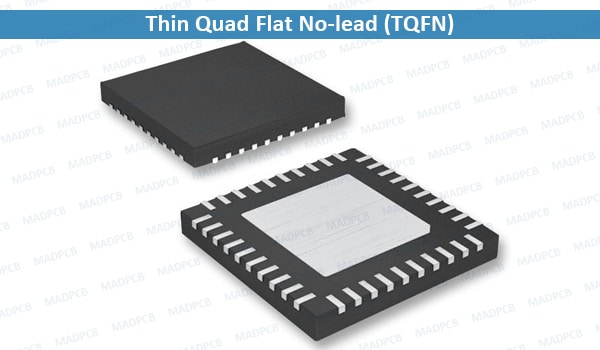
Thin Quad Flat No-lead (TQFN)
Typical pad counts range from 8 to 68. The maximum body thickness of this packages is 0.8mm, and the typical thickness is 0.75mm. The body sizes range from 3mm2 to 10mm2. The pad pitch (distance between pads) used is usually either 0.4mm or 0.5mm.
| Properties of Some Thin QFN Examples | ||||
| Part Number | No. of Pads | Body Size | Body Thickness | Pad Pitch |
| TQFN-8 | 8 | 3 x 3mm | 0.75mm | 0.65mm |
| TQFN-16 | 16 | 3 x 3mm | 0.75mm | 0.4mm |
| TQFN-20 | 20 | 4 x 4mm | 0.75mm | 0.5mm |
| TQFN-24 | 24 | 4 x 5mm | 0.75mm | 0.5mm |
| TQFN-36 | 36 | 6 x 6mm | 0.75mm | 0.5mm |
| TQFN-48 | 48 | 6 x 8mm | 0.75mm | 0.5mm |
| TQFN-56 | 56 | 7 x 7mm | 0.75mm | 0.4mm |
| TQFN-68 | 68 | 10 x 10mm | 0.75mm | 0.5mm |
Thin QFN package provides superior electric and thermal performance over the standard QFN package and is very suitable for high current DC to DC converters.
- Superior electrical and thermal performance compared to QFN and leaded plastic packages.
- Easy to PCB layout.
- Small footprint results in significant PCB space savings.
- Can utilize the standard surface mount assembly technology.
- Proved Board-Level Reliability per IPC-9701 Performance Test Methods and Qualification Requirement for Surface Mount Solder Attachments.
TFQN Rework Process
Here, we do not talk about TFQN PCB assembly, but its rework. For the TQFN parts, if there is any defect underneath the package, the whole package has to be removed. Rework of TQFP packages can be a challenge due to their small size. In most applications, these parts will be mounted on smaller, thinner, and denser PCBs that introduce further challenges due to handling and heating issues. Since reflow of adjacent parts is not desirable during rework, the proximity of other components may further complicate this process. Because of the product dependent complexities, the following only provides a guideline and a starting point for the development of a successful rework process for these packages.
Usually, the rework of TQFNs includes the following steps:
- Thermal profiling;
- Removal of defective component;
- Site redress;
- Solder paste replenishment;
- New component placement;
- Reflow soldering;
- Final inspection
Want to know more about the details of the whole rework processes, or in any demand of PCB manufacturing, assembly and design, just feel free to contact us.