What’s VQFN Package?
Very-Thin-Profile Quad Flat No-Lead Package (VQFN) is a near chip-scale plastic encapsulated package. It provides on the package bottom side perimeter pads and also a large die pad, which is typically also soldered to the printed circuit board (PCB) to get an optimum of electrical and thermal performance and board level reliability.
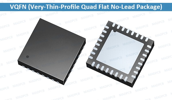
VQFN (Very-Thin-Profile Quad Flat No-Lead Package)
Features
- Optimized electrical performance with short leads
- Enhanced thermal performance through exposed die pad structure
- Leads and exposed die pad with solder plating
- Small footprint, thin package
- Package outline according JEDEC MO-220
VQFN PCB Design
Generally, the PCB design and construction is a key factor for achieving a high circuit board assembly yield and also sufficient reliability. Examples are PCB pad designs of for the perimeter lands and for the large central thermal pad, which is generally recommended to be soldered to the PCB for having optimum thermal, electrical, and board level reliability performance. Also, the via design and board finish have to be considered.
Additionally, studies at the customers may be necessary for optimization, which take into account the actual PCB manufacturer’s manufacturing capability, SMT house’s PCB assembly process, and product specific requirements.
PCB Pad Design
The extension of the PCB pad helps to develop a solder joint fillet at the side wall of the VQFN land. However, this cannot be guaranteed, as this area is not plated. Other influencing factors for fillet formation are package exposure to environment, solder paste material, and reflow process. If fillets are formed, this will additionally be beneficial for solder joint reliability.
The VQFN packages have got a central die pad. The surface plating is the same as for the outer package pads. In most applications the die pad allows to transfer a large amount of heat into the PCB to achieve higher thermal performance. Therefore, it should be soldered to the board onto the thermal pad. This also increases solder joint reliability and for some applications/products the electrical performance. We recommended to use die pad size on the QVFN package as maximum thermal pad size on the PCB. Slightly smaller size of the thermal pad is also possible.
Vias in Thermal Pad
A typical via hole diameter for such thermal vias is 0.3mm. The number of vias in the thermal pad depends on the thermal requirements of the end product, the power consumption of the product, the application, and the construction of the printed circuit board. However, an array of thermal vias with pitch 1.0-1.2mm can be a reasonable starting point for most products/applications for further optimization.
If the vias remain open during board manufacturing, then solder may flow into the vias during VQFN boar assembly (solder wicking). This could have the effects of large voids in the thermal solder joint under the die pad, lower stand-off (which is controlled by the solder volume between package die and thermal pad on PCB), and/or solder protruding from the other side of the board, which may disturb a second solder paste printing process on this other board side. If necessary, the solder wicking can be avoided by plugging of the vias (filling with epoxy) or tenting the via with solder mask (e.g. with dry-film solder mask). Via tenting shall be done from top, because with via tenting from bottom side voiding rate is significantly higher).
PCB Pad Finishes
The solder pads must have good wettability to the solder paste. In general, all finishes listed in the page of Surface Finish are well proven for SMT assembly, but especially for fine pitch applications, like for VQFN packages, the quality of the plating/finish gets more important. Because of the uneven surface of HASL finish, lead-free or lead containing HASL is less preferred for VQFN assembly (especially for pitch < 0.65mm) compared to completely “flat” plating, like Cu-OSP or electroless Sn or NiAu.
It is not possible to give a definite recommendation for PCB pad finish. It also depends strongly on board design, pad geometry, all components on board, and process conditions.