PCB panelization guidelines in this blog set out best practice to reduce your PCB costs and to minimize the risk of errors arising during manufacturing. We talk completely straight about our processes and pricing model. If you’re new to the industry, or just looking for hints on how to lower your PCB costs, keep reading and perhaps you’ll learn something new. Nothing in this article is rocket-science, it’s really a matter of some common-sense math.
Table of Contents
Free Panel Creation
Many of our customers are contract electronics manufacturers (CEM’s). We have a lot of experience in setting up arrays for automated assembly. We can follow your array specifications or we can set one up for you. We will score where possible and tab-rout (rout and retain) where it isn’t. Many assemblers have guidelines as to how they prefer arrays to be constructed. Check with your assembler if they have size limitations or preferences regarding rail placement, tooling holes, or fiducials.
- Panel data provided by the customer: no extra charge.
- Panel composed by MADPCB, free!
- Once the boards are too small or without fixing holes, we will suggest to create panel, and confirm with you whether
separation is needed before delivery, free creation and separation!
- Free charges if you want us help to compose different circuit boards into one panel. (The setup cost will be only half for the extra one).
PCB Panel Types Examples
Mechanical Processing and Design Parameters
Scored Panel: Scoring is the preferred choice for two reasons. Scoring has the advantage of a more consistently smooth board edge, and it wastes less material, which can mean cost savings especially for larger quantities or high layer count printed circuit boards where every square inch counts.
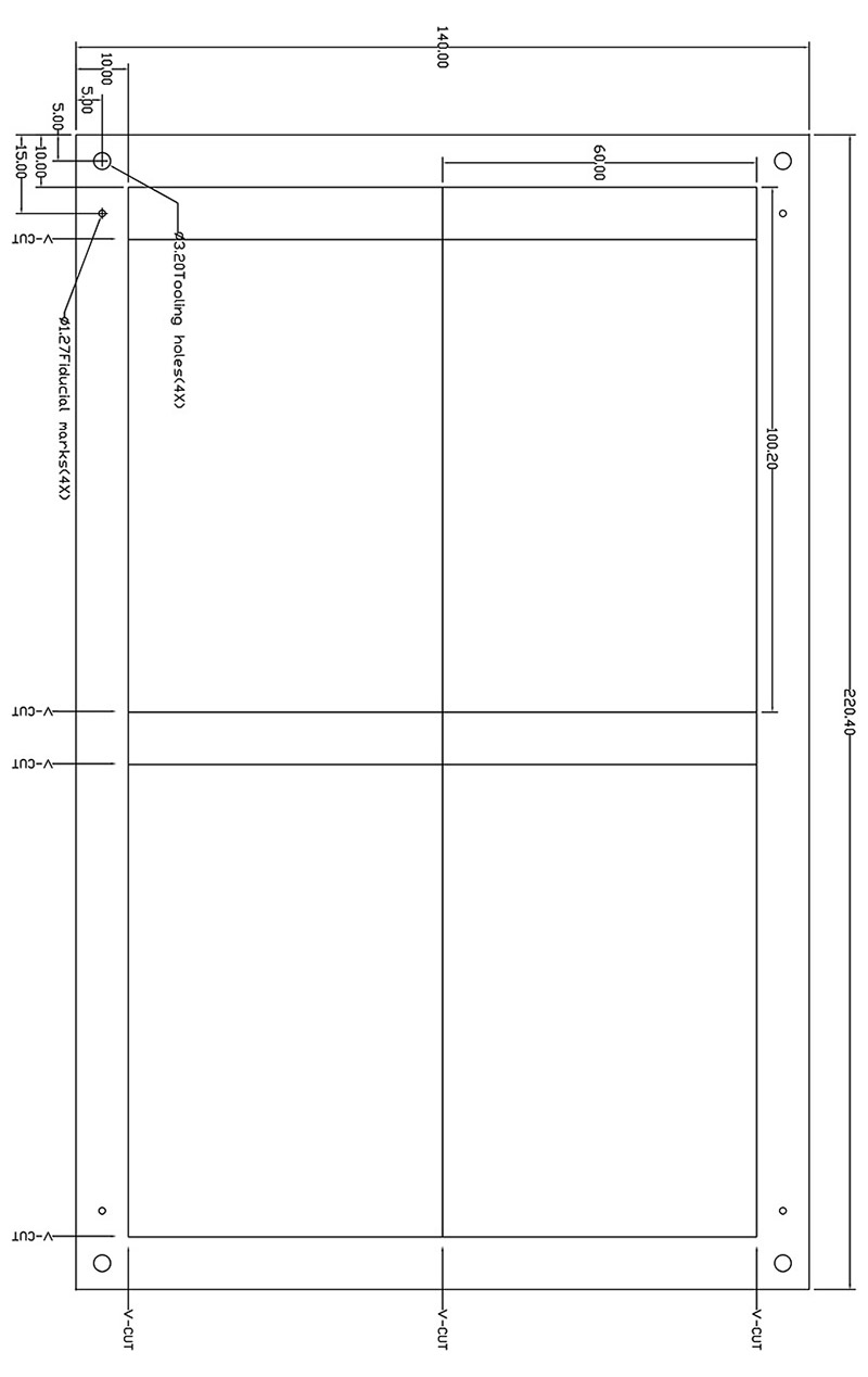
We recommend the use of a minimum panel border of 5.00 mm base material. Two parallel edges are added along the two longest sides and there will be no space between the boards. The scoring will be made along the shared board outline. Scoring is performed only parallel to the x- and y-axes, not diagonally. Because scoring runs all the way across the array in a straight line, the board outline should be straight for scored arrays.
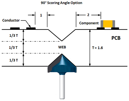
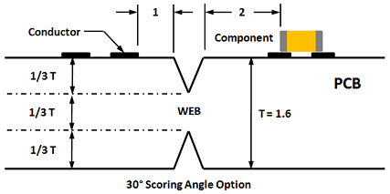
The score depth is approximately 1/3 of the total material thickness. Score lines will be made on the top and bottom sides of the PCB. This will leave a remaining web of material equal to approximately 1/3 of the total thickness of the board. If your board is .062″ thick, the remaining material will be ~.021″. We recommend using scoring technology only for panels with a circuit board thickness of at least 1mm (stability). However, in fact V-Groove scoring inner web material can range from 0.15 mm to 0.4 mm for panel separation depending on the length of the score. If the score length is less than 25 mm, it can have a web thickness of 0.15 mm and scores that are 100 mm long can have a web thickness of 0.25 mm and scores that are longer than 100 mm can have a web thickness of 0.4 mm. These values are just guidelines and should be discussed with your assembly shop to confirm the web thickness for your printed circuit board design.
Standard PCB material is essentially fiberglass. Even though your board is scored, it will still be sturdy so be careful when separating the boards. Expect some amount of flexing before the score line will give. Some fiberglass strands are common along a scored edge. A quick bump with a belt sander will take care of any rough areas.
Fig.1 illustrates the 90° scoring option. It is important that all conductors be routed within a minimum distance of 1 mm from the top of the scoring edge to prevent damage during de-paneling. The inner layer planes should be pulled back 1 mm from the V-groove. The PCB designer should collaborate with the PCB fabrication shop on the V-groove angle option that they use.
Note: all dimensions in this paper are in millimeter units.
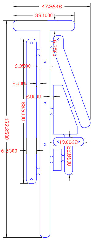
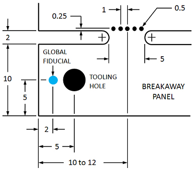
Tab Routing (Milling with bridges to break out). Consider tab routing when your design has an irregular shape or if you need space between your boards to allow for overhanging components. Our default is to add a 0.1″ (2.0mm) gap between the boards to allow the router bit to pass between them. Small tabs of material will remain to hold the boards in place. To make separation easier, we can add small non-plated holes to the tabs called ‘mouse bites’ to perforate the tab. The breakaway tab closest to the PCB corner should be located between 10 mm and 12 mm from the edge to reduce sagging during reflow or wave soldering. It is also preferred to have at least one tab per side. If the PCB placement is too dense for a Tooling Hole, then it should be placed on the breakaway tab. See Figure 1 for the optimized breakaway tab solution.
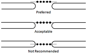
One important aspect is to have a clean edge after the breakaway tab is removed. Slight inset of perforation is preferred because it provides an edge which requires little to no additional labor to clean up. Figure 2 illustrates the perforation location preferences.
The spacing between breakaway tabs can range from 60 mm to 90 mm, but we recommend 77 mm from center to center as shown in Figure 3. Try not to exceed 100 mm between tabs and try to evenly space them apart.
The plane pull-back should be at least 1 mm from all slots and perforation holes. All trace routing needs to be over a plane for clean return path so keep all routing 1 mm from all slots and perforation holes. Keep components 2 mm – 3mm away from the routed slots. These rules help prevent components or trace damage during the de-paneling process. See Figure 4 to define the keep-out areas in the PCB layout.
Tab routing is more precise than V-groove scoring and edge surfaces are smooth. The breakaway tab points require consideration for additional smoothing if necessary to comply with the fabrication drawing note regarding smooth edges. The dilled perforation provides a low stress break point on the tab and if the hole pattern is recessed within the printed board edge, secondary sanding or grinding can be avoided.
A mixture of both: A mix of scoring and tab routing can be used when some board sides are straight, which can be scored, while irregular sides must be tab routed. It is not recommended to substitute perforation holes with a V-groove score as it does not provide a durable tab that will withstand handling. V-groove scoring can however be used in place of routing, but requires board edge grinding to smooth the surface. It is important to note that only the 1/3 depth rule applies to “Breakaway Panels”.

