Table of Contents
FPC Coverlay in Flex Circuits?
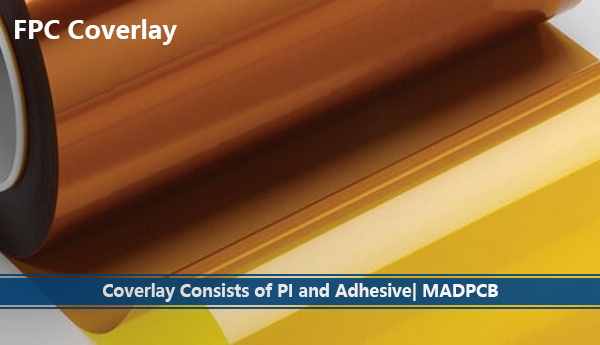
FPC Coverlay consists of a solid sheet of polyimide with a layer of flexible adhesive. Coverlay plays the exact same function as a solder mask on rigid boards but only for flexible printed circuit boards (PCBs). Conventional solder masks have only a limited bendability, so for flex circuits that require greater bendability, coverlay is bonded (glued) on to encapsulate and protect the external copper circuit layers of a flexible printed circuit (FPC).
Different from rigid PCB solder mask, coverlay is typically supplied in a roll form, sometimes in sheet and cut to size. From there, the coverlay openings needed may be drilled, routed, punched, or laser cut depending on the complexity of the flex PCB design and feature sizes. Once the pattern is created, the film is then aligned to the copper circuit layer and pressed under heat and pressure, over time, to cure the adhesive to complete the coverlay bonding.
Drilling is the most common method to create the feature openings and there are a few design related considerations to keep in mind:
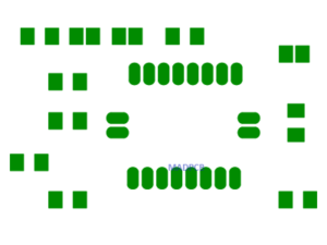
- Mechanical NC drill bits are round, so the FPC manufacturer will be working with a round or oval size hole in the coverlay film and often these are covering square surface mount pads.
- A larger annular ring will be needed to accommodate both the adhesive squeeze out that occurs during the pressing operation and manufacturing tolerances associated with drilling.
- The minimum web thickness will also need to be large enough to ensure a strong enough adhesive bonding and to avoid de-lamination risk.
Sometimes, for better electrical isolation between inner copper layers in multilayer flexible printed circuits, MADPCB uses TPI (thermoplastic PI) to replace coverlay.
Common Coverlay Configurations
| Coverlay Consists of Adhesive and Polyimide (PI) | ||
| Name | Polyimide Thickness μm (mil) |
Adhesive Thickness μm (mil) |
| 13/15 | 13 (0.5) | 15 (0.6) |
| 13/25 | *13 (0.5) | 25 (1.0) |
| 25/25 | 25 (1.0) | 25 (1.0) |
| 25/35 | 25 (1.0) | 35 (1.4) |
| 25/50 | 25 (1.0) | *50 (1.0) |
How to Choose the Correct Coverlay for Your Flex PCB?
- Min Bend Radius Requirement: Thinner coverlay may be required to meet tight bend requirement.
- Finished Copper Weight of the External Layers: Min of 1mil (25μm) of adhesive is required per OZ (35μm) to ensure complete encapsulation. E.g. 1oz finished copper requires 1mil adhesive at least.
- Cost: Thinner or thicker adhesive are more expensive.
- Dielectric Withstanding Voltage (rare)
Component Feature Openings
The disadvantage of using coverlay film is that it must normally be cut or drilled, and can no be developed like LPI solder mask. Thus, only larger structures in a rectangle shape are possible, as well as small aperture exemptions that are always around drilled. For flexible PCBs with fine pitch SMD component features, coverlay is only for limited use.
Features formation methods on its opening include drilling, routing, laser cutting, knife cutting, or punching & die sets, and any of their combination. The exact method(s) is dependent upon the feature shape, size, complexity, and quantity of parts being manufactured. Then, this brings additional considerations beyond Flex LPI:
- Larger Min Annular Ring to Exposed Feature Requirements: allows for material and manufacturing tolerances and potential adhesive squeeze out during lamination.
- Larger Min Web Thickness between Adjacent Features: Prevents easily damaged thin sections or webs; Allows for sufficient adhesive to ensure proper lamination and copper circuitry encapsulation.
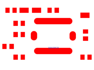
In flexible PCB designs with higher density SMT and/or PTH features and if the design allows, it is required to combine multiple feature openings into larger “ganged” openings to accommodate the above features. While, sometimes it allows to use both coverlay and LPI soldermask. The solder mask is used to cover the spaces between small features, coverlay is used to cover remaining areas, and exposure the features.
Apply Coverlay and LPI Soldermask to Specific Areas with Stiffeners
Some rigid-flex printed circuit boards (PCBs) due to their density, complexity, and/or component requirements may require the use of both coverlay and LPI soldermask. Both are selectively applied to specific areas of the part and provide benefits of bother materials within one design. The PCB manufacturing files are created to ensure that the two materials overlap within the rigidized area(s). This results in a complete encapsulation of the circuitry without the creation of mechanical bend stress concentrators in the flexible areas. If this were allowed the reliability of the part may be compromised. While this methodology adds some cost, the rigid-flex design may mandate it and/or the benefits outweigh the added cost. There are two common configurations of coverlay and LPI soldermask:
- Either apply LPI solder mask in rigidized component areas and coverlay in the flexible sections.
- Or add selective webs of solder mask in ganged coverlay openings.
Additional Considerations when Apply Coverlay
FPC and rigid-flex board designs that have one or more of the following may require the use of coverlay throughout in specific areas of layers, because the following materials may not sufficiently adhere to LPI soldermask and pass IPC quality control requirements.


