What’s CGA Package?
CGA (Column Grid Array) IC Packages are made with non-collapsible solder columns for surface mount soldering on printed circuit board (PCB). Most CGA packages have large ceramic substrates (also called CCGA) 21mm to 52.5mm. It is noteworthy to mention that there is increasing interest in replacing solder balls on (organic) Plastic Ball Grid Arrays (PBGA) with solder columns. CGA packages are typically 1.0mm or 1.27mm pitch. Experimentation suggests the feasibility to use solder columns for narrower pitch CGA packages down to 0.8mm and eventually smaller pitches.
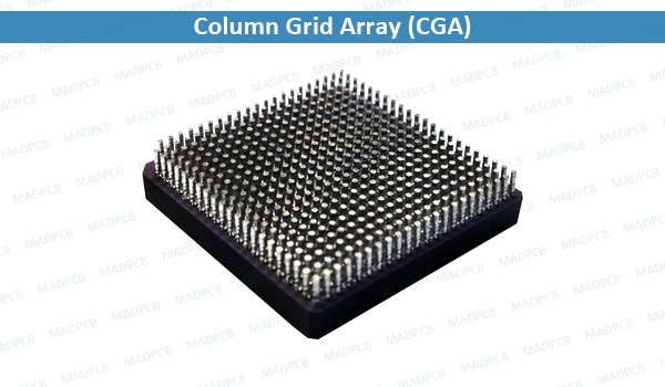
Column Grid Array (CGA)
Solder columns absorb CTE mismatch between the IC package and the circuit board. CTE mismatch is inherent due to joining different material properties between the IC package and the PCB board. The CTE mismatch differential between a ceramic IC package and PCB is 10ppm/oC in the X/Y axis. CTE mismatch rises above 50ppm/oC in the Z-axis as temperatures exceed the Tg rating of the PCB. As the IC package increases in size, the differentials of CTE mismatch become more significant, especially when the package is subjected to repeatedly wide temperature cycles from -40oC to +125oC.
Stress due to CTE mismatch results in eventual delamination and catastrophic electrical failure between a large ceramic BGA IC package and the PCB. The corner pads are most prone to fail as well as the corners directly under the silicon die mounted on (or in) the package.
Solder columns (nominally 2.2mm long) shown on the ceramic package provides more compliancy than solder balls to reduce stress caused by CET mismatch. Tall solder columns absorb stress and increase solder joint reliability under harsh operating conditions.
Older style solder columns are constructed of high melting temperature Pb90/Sn10 wire (or cast) without copper wrapping. Such “plain” columns tend to decrease electrical performance, especially at higher frequencies. Columns increase the overall package profile height, as compared to BGA components.
Solder columns are available in a variety of lengths from 1.0mm to 2.54mm. However, solder columns of 2.21mm nominal length tend to be the industry norm for most CGA packages. Longer columns, such as 3.81mm, are useful for raising IC packages with bottom mounted decoupling capacitors off the circuit board.
Ideally, the diameter of the solder column should be roughly 75% of the landing pad diameter to allow a proper annular solder fillet to form around both ends of solder columns after joining the IC package to the PCB circuit board. Solder columns are available with diameters as small as Ø0.20mm and as large as Ø0.56mm (Ø0.89mm for certain applications).
Solder columns have been successfully attached to organic PBGA substrates. Ø0.50mm diameter solder columns tend to be the industry norm for 1.0mm and 1.27mm pitch ceramic IC packages. Smaller size solder columns with Ø0.38mm diameter are required for commercial off-the-shelf (COTS) 1.0mm pitch organic substrates (PBGA without solder balls), since most 1.0mm pitch PBGA packages have Ø0.50mm solder mask defined pads (SMD). Even smaller solder columns Ø0.25mm ~ 0.30mm diameter are required for 0.8mm pitch PBGA packages, depending on the diameter of the solder mask defined pads.
Solder columns are constructed of high melting point solder alloys. Solder Columns do not collapse during reflow to the PCB circuit board. Typically, Military/defense/aerospace applications require eutectic Sn63/Pb37 solder paste; however, commercial applications require SAC305 lead-free solder pastes.
At the time of this writing, high lead bearing solder columns such as Pb90/Sn10 and Pb85/Sn15 are exempt from RoHS per IPC-1752A 7(a) published March 2011.
Solder columns are constructed of high melting temperature alloys, including Pb80/Sn20, Pb85/Sn15 and Pb90/Sn10, wound with an outer layer of oxygen free (OFHC-101 or alloy CDA101) copper. The thin layer of copper ribbon (0.025mm to 0.050mm thick) is spirally wrapped around the column. Columns are coated with eutectic Sn63/Pb37 to cover the copper ribbon and form a lap joint between the copper to the solder column.
Pb90/Sn10 solder columns constructed with electroplated Cu copper shield provides 30% lower thermal resistance than copper wrapped columns to conduct heat away from the bottom of the IC package to the ground-plane of the circuit board. The thickness of the Cu copper is 0.025mm to 0.050mm. A thin coating of Sn60/Sn40 covers the exterior Cu copper.
Micro-Coil Springs, introduced by NASA, provide an alternative to traditional solder columns. The base material is Beryllium-Copper (Be-Cu) wire. The wire is electroplated with a choice of Pb60/Sn40 or Ni-Au. The NiAu gold (Au 2.5µm maximum) plated version provides a lead-free solution when combined with SAC305 fillets. Coil size is Ø0.50mm (O.D.) diameter by 1.27mm long (free-load length) is use with 1.0mm pitch ceramic IC packages with Ø0.80mm pads. A smaller coil with Ø0.40mm (O.D.) diameter and 1.0mm length is used when attaching to organic PBGA substrates with Ø0.50mm solder mask defined pads.
Graphite tool-sets are required to attach solder columns to CGA packages. The tool-sets are designed for specific size, pad counts and ceramic and organic PBGA style Land Grid Array (LGA) substrates. The tool-set includes a bottom graphite to hold the LGA substrate and a mating top graphite to align Flip-Pack cassettes pre-loaded with columns. Use a pallet to hold the bottom graphite during solder paste stencil printing. An entry level tool-set can process volumes up to 500 CGA packages per month. You can increase throughput by adding more bottom graphite bases and top graphite tools to 10,000 packages per month.