What Is Crosstalk in a PCB?
Crosstalk is an undesired electromagnetic coupling among the traces on a printed circuit board (PCB), even though the traces are not in physical contact with each other. Electromagnetic field disturbance can take place in PCBs due to external interference. Crosstalk occurs when there is capacitive and inductive of power from the aggressor signal to the victim signal (typically, two adjacent traces) in terms of interference of electric and magnetic fields.
- Victim Line: also, victim trace, the net or transmission line where a crosstalk signal is induced
- Aggressor Line: also, aggressor trace, the net or transmission line that induces the crosstalk signal in the victim
The electric field is coupled via mutual capacitance between the signals. On the other hand, the magnetic field is coupled via mutual inductance between the signals. Traces running parallel on the same layer or running parallel vertically between two layers are susceptible to crosstalk.
Negative Crosstalk Effect
Crosstalk is one of those more complex signal integrity problems, and it is sometimes misunderstood. All crosstalk arises due to unintended coupling through the electromagnetic field, but there are different types of crosstalk to consider in any PCB design. Crosstalk can never be eliminated, but it can be reduced to the point where it does not affect signal quality at the receiver.
For digital boards operating at high speeds and high data rates, crosstalk can be hugely problematic and difficult to pinpoint, simply because there can be so many nets involved in producing crosstalk simultaneously. Analog boards have fewer signals and crosstalk can be identified easily, but it can be difficult to eliminate down to an acceptable level as analog components and traces react so strongly to external noise. Let’s look at the different types of crosstalk in your PCB and some steps you can take to eliminate them.
Crosstalk in circuit boards generates undesirable effects that affect clock, periods signals, system-critical nets like data lines, control signals, and I/Os. Additionally, the affected clock and periodic signals create serious functionality concerns for working PCB and assembly components. Due to the negative effect, the voltage and current levels outreach the threshold level of the logic devices. This can be interpreted as a false logic state when it reaches the receiver. A designer needs to work smartly to avoid the error caused by these erroneous logic states. Crosstalk can also affect analog signals by adding noise. This noise could come through the power rails.
Types of Crosstalk in a PCB
All crosstalk occurs between a victim line and one or more aggressor lines, and there are several terms used to describe types of crosstalk as following:
- Far-end crosstalk (FEXT): This is the crosstalk signal measured at the receiver end of a cable or transmission line.
- Near-end crosstalk (NEXT): This is the crosstalk signal measured at the transmitter end of a cable or transmission line.
- Power-sum NEXT and FEXT (PSNEXT and PSFEXT): These are not a different type of crosstalk, these terms simply refer to the way in which crosstalk is quantified. In this case, it’s done in terms of absolute or relative power.
- Alien crosstalk (AXT): This term is used in the telecommunications industry to describe crosstalk between twisted pair wiring, but it is also used to describe crosstalk in PCBs for telecom systems.
- Power-sum equal-level crosstalk (PS-ELFEXT): This is basically equal to PS-FEXT + PS-NEXT.
- Forward and backward crosstalk: This just tells you the direction a crosstalk signal travels along a transmission line. Forward crosstalk propagates in the same direction as the aggressor signal, while backward crosstalk propagates in the opposite direction.
Crosstalk and Coupling Mechanisms
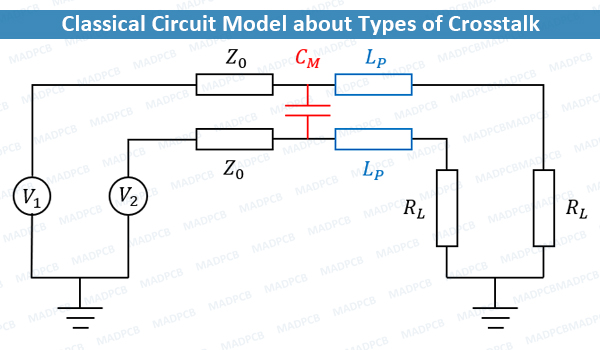
The circuit diagram below shows how circuit theory is used to model different types of crosstalk. In this diagram, there is some parasitic capacitance between the two traces, which exists due to broadside coupling between the traces. Because each trace is a loop of conductor, each trace acts like an inductor and has some parasitic inductance. The two parallel inductors have some mutual inductance, which defines the strength of inductive coupling between the two traces.
The capacitive coupling is not just meant to show the equivalent capacitor created by the edges of the traces, although this does contribute to the mutual capacitance. The native capacitance of each trace and the broadside capacitance combine to give the total mutual capacitance; they are all in series and coupled back to the ground plane.
When crosstalk occurs and is observed as a snapshot in the time domain, it is difficult to differentiate capacitive and inductive contributions to crosstalk. This is why we have FEXT and NEXT measurements; they basically allow you to quantify forward and backward crosstalk. Let’s look at how these coupling mechanisms produce the two types of crosstalk in a PCB.
Forward or Backward?
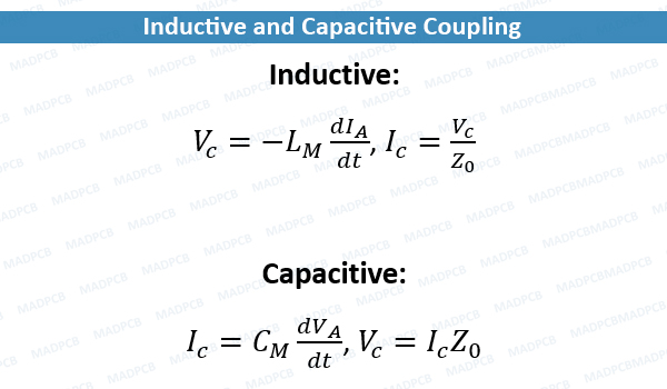
When an analog signal oscillates, or as a digital signal rises along the length of a trace, the changing current along the signal generates an oscillating magnetic field. The oscillating magnetic field then generates a changing magnetic flux within the cross section of the victim trace. Thanks to Faraday’s law, this induces a back EMF in the victim trace. In other words, the voltage signal created in the victim points opposite to the signal in the aggressor. Therefore, the Inductive coupling generates backwards crosstalk on the rising signal edge, and it generates forward crosstalk on the falling signal edge.
What about capacitive coupling? This is a bit more complicated in that you need to consider the distributed nature of the line. When the voltage on the aggressor line changes, a displacement current is induced in the victim trace. In this situation, the displacement current is only induced in the victim within a certain region (called the coupling length, more on that below). The displacement current then moves away from the point where the signal is induced along the line, i.e., towards the transmit and received ends.
Note that, for digital signals, the two lines act like a capacitor that needs to charge when there is a potential difference between the aggressor and victim lines. However, this charging effect occurs on the order of microseconds, so any stream of digital aggressor signals faster than ~1 MHz will induce glitches that appear on the victim with similar timescale.
Coupling Region
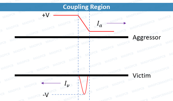
Note that both types of crosstalk only occur within a certain region that exists between the coupled aggressor and victim. Remember that a wave travelling on a transmission line is extended out over some distance, which depends on the dielectric constant of the substrate. Because the aggressor signal only changes within a certain portion of the aggressor trace, the crosstalk signal will only be induced in a small region in the victim trace. This is called the coupling region, and it is the region over which the signal is changing (see the above equations). The image below shows the coupling region for the rising edge of a digital signal on a pair of coupled transmission lines.
Note that forward and backward crosstalk can exist on a victim line simultaneously, which is why we care more about measuring NEXT and FEXT than about tracking forward or backward crosstalk. Once a summed crosstalk signal reaches the transmit or receive ends of the line, it can be measured as either NEXT or FEXT, respectively. With the right high speed layout practices and stackup design techniques, you can reduce crosstalk between different portions of your design. Here, we’ve only addressed single-ended crosstalk, but the same effects occur in differential pairs. I’ll get into more depth on crosstalk in analog systems and differential crosstalk in the future.
Crosstalk Reduction Practices in PCB Design
So now that you understand a bit about crosstalk, how do you guard against it in your PCB designs? The key thing to reduce but not remove crosstalk is that it occurs everywhere, it’s the largest between parallel signal lines.
The best way to reduce crosstalk is to exploit the very parallelism that leads to its creation by closely coupling the return path to ground to your high-speed signals. Since the return path is equal in magnitude but opposite in direction, the fields cancel out and reduce crosstalk.
Another way to ensure signal integrity is to use differential signaling, where two voltage lines equal in magnitude but opposite in polarity are used to create a single high-speed data signal. Since the actual data signal is taken as a difference between the voltages of the two voltage lines at the receiver, and because electromagnetic noise tends to affect both lines equally, the signal itself remains perceptible even in the presence of external noise.
Here are some quick summaries of PCB routing tips for reducing crosstalk:
- Reduce the length that two lines are allowed to run in parallel.
- Be sure to have solid return paths where possible.
- Use differential signaling where applicable.
- Use guard traces with vias connected to ground.
- Keep high-speed signals, especially clock signals, isolated from other traces where possible.
- Keep traces in adjacent layers perpendicular to each other.
At MADPCB, we regularly manufacture, assemble and design high speed PCBs which are sensitive to different types of crosstalk. We know how to create a high quality, fully manufacturable PCB layout for your system. We’re here to help electronics companies design modern PCBs and create cutting-edge technology. We’ll make sure your next layout is fully manufacturable at scale. Contact MADPCB for a consultation.


