Fan-In Wafer-Level Package (FI-WLP)
Fan-In Wafer-Level Package (FI-WLP) refers to the technology of packaging an integrated circuit (IC) at the wafer level, instead of the traditional process of assembling individual dies into packages after dicing them from a wafer. FI-WLP technology is an extension of the wafer fabrication process and uses the traditional fabrication processes and tools. A redistribution layer is used to connect device I/Os to bump (ball) locations on top of the die surface. The bumps are arranged in an array pattern that is compatible with traditional printed circuit board (PCB) assembly process. The bumps provide the interconnection to the application. FI-WLP is a true Chip-Scale Package (CSP) technology, because the resulting package is the same size as the die. Wafer-Level Package (WLP) technology differs from other Ball-Grid Array (BGA) and laminate-based CSPs in that no bond wires or interposer connections are required. The figure 1 shows typical FI-WLPs.
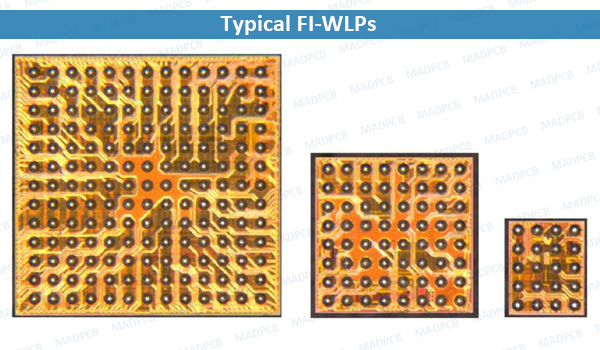
Typical FI-WLPs
Fan-Out Wafer-Level Package (FO-WLP)
Fan-Out Wafer-Level Package (FO-WLP) is an enhancement of standard WLPs, enabling a greater number of I/O connections. This package involves dicing chips from a silicon wafer, precisely positioning the known-good-die on a “reconstituted” or “carrier” wafer / panel, which is then molded. This is followed by making a redistribution layer on top of the die and the molded area, and then connecting bumps on top. Redistribution of I/Os to the mold compound regions outside the periphery of the die allows a greater number of I/O connections compared to an FI-WLP. The figure 2 shows typical FO-WLPs.
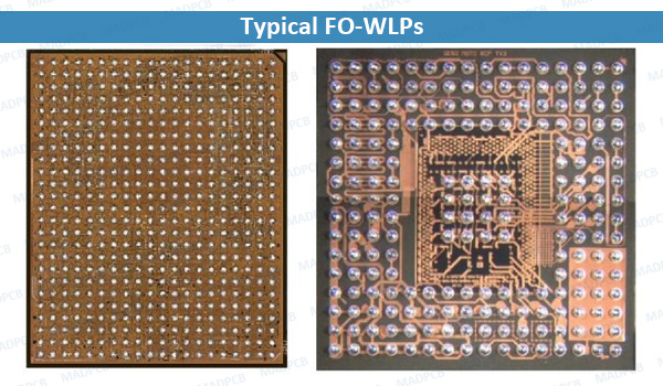
Typical FO-WLPs
WLPs can have three distinct constructions:
- Repassivation
- Redistribution
- Direct bumping
Repassivation: The I/Os on the die are designed in such a way that they are already at the bump position. A repassivation layer is added on the bond pad, followed by the Under-Bump-Metallization (UBM) and the bump. See figure 3:
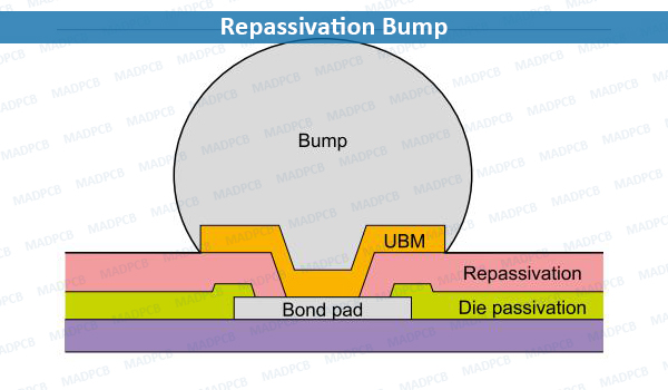
Repassivation Bump
Redistribution: The I/Os on the die are relocated to the correct bump locations with a redistribution layer. Two repassivation layers are used. See figure 4.
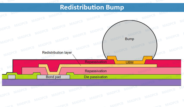
Redistribution Bump
Direct Bumping: The UBM is deposited directly on the wafer passivation without a compliant layer in between. See figure 5. This construction has limited use.
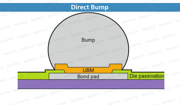
Direct Bump
Notes
- FO-WLP uses only redistribution type of construction
- Some FI-WLPs are over-molded or have a back-side protection coating
WLP packages are in various sizes, thicknesses, I/O layouts and standard minimum ball pitches of 0.35mm, 0.40mm and 0.50mm. The physical outlines of a WLP depend on the actual die size.
Are you finding a reliable quick-turn PCB and assembly supplier? Contact us and have a quick quote now for your turnkey PCB assembly projects.