What Is PCB Shield?
PCB Shield is the mechanical approach of adopting conductive, magnetic or both materials to prevent EMI in the electronic device. Mechanical shields are closed, metal cans, like brass, nickel silver and stainless steel, which connected to the ground of the printed circuit board (PCB). They effectively decrease loop antenna sizes, and absorb and/or reflect some of the radiation. This is similar to that using EMI shielding film in flexible printed circuits (FPCs).
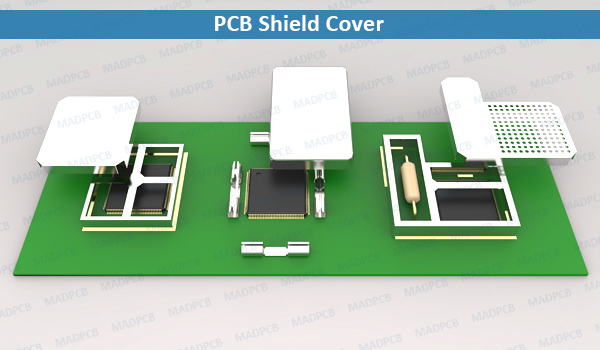
PCB Shield Cover
Shielding Effectiveness (SE)
The shielding effectiveness (SE) is typically defined as the ratio of the magnitude of the incident electric wave (E1) to the magnitude of the transmitted attenuated wave (E2):
SE (Db) = 20 log E1/E2
The higher SE (Db) number equals to better shielding material. Most high-frequency shielding issues are the result of gaps of slots in the shielding material, not usually the material itself.
Two shielding mechanisms are:
- Reflection (R): Reflection occurs when energy from the electromagnetic wave encounters the shield and is reflected back.
- Absorption (A): Absorption is what happens when non-reflected energy from the wave is absorbed in the shield with only the remaining energy emerging from the other side.
These two effects (or losses) combine to form the total shielding effectiveness, often expressed as
SE(Db)=R(dB) + A(Db)
There is a third term sometimes added to this equation, called
- Re-reflection (B): Re-reflection could decrease the shielding expected however it only occurs in extremely thin shields.
Of course, B term can be ignored in most electronic devices which are constructed of shielding material strong enough to support its own weight and the shield can obviously be considered thick.
There are a couple of other key points regarding reflection and absorption losses that you take note of.
Reflection Loss
Higher conductivity materials result in higher reflection losses and that the distance of the EMI source from the shield also affects reflection losses due to what the impedance of the electromagnetic wave is at certain points in space. A higher wave impedance, combined with lower shield impedance (in Ohms per Square) results in a higher reflection loss. Because the primary reflection occurs at the first surface of the shield in the case of electric fields, even very thin materials provide good reflection losses.
For a plane wave (an electromagnetic field located in the far field at a distance of approximately 1/2π, where I = wavelength) that is entering a shield at normal incidence, the following equation is used to determine R:
R = 20 log ZW/4ZS (dB)
ZW = impedance of wave prior to entering shield
ZS = impedance of shield
As the angle of incidence of the impinging electromagnetic wave increase so does the reflection loss. A lower shield impedance also results in a greater reflection loss and vice versa.
In the near field of the electromagnetic wave (distance <1/2π), it’s imperative to know the characteristics of the source, the highest frequency of interest until the separation distance 1/2π, beyond which the reflection loss is the same as for a plane wave. In contrast, the reflection loss of a magnetic field increases with frequency until the separation becomes 1/2π.
Because an understanding of the above information is important in the determination of reflection loss, then to determine the characteristics of the source (electric – wave impedance >377Ω, magnetic – wave impedance <377Ω, or plane – wave impedance of the medium or free space = 377 Ω) during troubleshooting activity.
Absorption Loss
The material’s permeability (μ), conductivity (r), thickness (t) and frequency of the electromagnetic wave all contribute to skin depth (SD) and therefore to absorption loss because A(dB) = 8.68 (t/SD). Skin depth is where electric current tends to flow on the outer surface of a conductor at higher frequencies and it is the depth where the field/surface current is attenuated by 37% or approximately 9dB. Another way t think about it is that the absorption loss in a shield one skin-depth thick is approximately 9dB and that doubling the thickness of the shield doubles the loss in decibels. Also, absorption loss (dB) is proportional to the square root of the product of the permeability times the conductivity of the shield material and this loss increases with frequency and as well as with shield thickness. Steel offers more absorption loss than copper of the same thickness.
The Effect of Apertures, Slots and Penetrations
When have a depth understanding of guidelines associated with adding apertures and slots and other penetrations to shields, inherent shielding effectiveness of the shield material at the high frequencies is of less concern that what the leakage is through the apertures used to carry signals in and out of the product. Aperture control is highly dependent on the maximum linear dimension and not the area of the aperture, the impedance of the electromagnetic wave and also its frequency.
- Keep slots shorter than one-twenties at least 20dB of attenuation.
- Shield or filter all cables that enter or leave the shielded enclosure and tie shields to the enclosure.
- Maintain electric contact across the seams of shielded enclosures in order to minimize leakage.
- If possible, limit the number of apertures as shielding effectiveness decreases proportional to the square root of their number.
- A large number of small holes produces less leakage than a large hole of the small total area.
- Shields do not have to be grounded in order to be effective.
Typical Attributes of PCB Shield Cans
- Small footprints;
- Low-profile configurations;
- Two-piece design (fence and cover);
- Through-hole or surface mount;
- Multi-cavity patterns (isolate multiple components using the same shield);
- Virtually limitless design flexibility;
- Ventilation holes;
- Removable covers for quick access to components;
- I/O holes;
- Connector cutouts;
- Enhanced shielding with RF absorbers;
- ESD protection with insulator padding;
- Reliable protection from shock and vibration using secure locking features between the frame and cover.
Typical Shielding Materials
A wide range of materials are generally available for shielding, including brass, nickel silver and stainless steel. The most common types are:
- Tin plated cold rolled steel (cheapest option)
- Tim plated copper
- Nickel silver
- Stainless steel
- Tin plated phosphorous bronze
In general, tin plated steel is the best choice for shielding below 100 MHz while tin plated copper is best above 200 MHz. Tin plating allows for the best soldering efficiency possible. Because aluminum on its own is not easily soldered to a ground plane with its heat-sinking properties, it is not generally used for PCB level shielding.
Depending on the regulatory burden of the end-product, all materials used for shielding may need to be RoHs compliant. In addition, if a product is intended for hot and humid environments, galvanic corrosion and oxidation may be of concern. If in doubt, check suitability of the shielding material with the supplier.