What’s TBGA Package?
Tape Ball Grid Array (TBGA) packages are a family of electronic chip carriers that utilize circuitized flex (tape) as the die carrier mounted to a printed circuit card or board (PCB). Previously this family of packages has been referred to by several designations, among them: Area Array Tape Automated Bonding (ATAB), Tape Ball Grid Array (TBGA), fleXBGA, Wire Bond TBGA (WB TBGA), Signetics TBGA (S-TBGA). TBGA is by far the most popular acronym utilized for this family of packages and adopted by the Joint Electronic Device Engineering Council of the Electronic Industry Association (JEDEC) for its standard package outlines. Since the chip carrier is circuitized flex, it has been suggested that these packages more appropriately be referred to as Flex BGAs (FBGA).
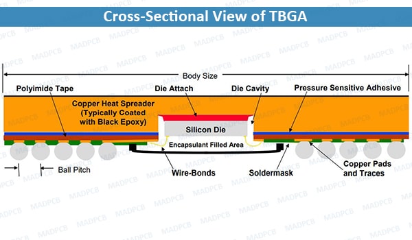
Cross-Sectional View of TBGA
Early applications of TBGA, in the range of 208 to 700 I/O (predominated two-level metal chip carriers), focused on the excellent electrical, thermal and reliability attributes of the package. Two-level metal TBGA is intermediate in cost to the other major types of BGA offerings, with ceramic being more and laminate less expensive. Thin polyimide flex substrates (100 to 125μm thick) also made TBGA the lowest profile BGA available. More recently, single-level metal wire bond and thermocompression bond designs have made TBGA cost competitive with laminate BGAs. Thin, light-weight overmolded designs are competing with conventional molded quad flat packs (QFPs) and address the needs of the portable consumer market; cellular phones, pagers, PC laptops, digital cameras, camcorders, etc. Packages with up to 96 I/Os are only 1.02mm from the ball grid seating plane to the component’s top surface, and up to 280 I/O only 1.0mm. Examples of some typical TBGA applications are given in following table.
| Typical TBGA Chip Carrier Users and Applications | |||
| User | Package I/O | P/N | Applications |
| Toshiba | 420 | TC220E TC240 |
ASIC (.3μm) ASIC (.25μm) |
| Fajitsu | up to 720 | CS71/CE71 | ASIC (.25μm) |
| Applied Micro Circutis Corp. | 208 | S2065 | EtherNet Switch/Tranceiver (1.25Gbps) |
| Broadcom | 352 | BCM5308 | Switch/Tranceiver |
| Motorola | 480 | MPC8260 | Power PC μP |
| Altera | 256 100 |
EPM7256A EPF10K100B |
Prog.Logic Device |
| VLSI | up to 672 | ASIC | |
| LSI | 240-736 | ASIC | |
| Vittesse Semiconductor | GaAs ASIC | ||
| NEC | 500 300+ |
VRC5074 CB-C10 |
RISC μP FPGA, ASIC |
| Texas Instruments | 64-240 | DSP | |
| Arithmos | 352 | ADI21/2200 | LCD Display Engine |
| Tri Quint | 208 | TQ8213/23 | ASIC Multiplexer |
TBGA chip carriers were initially used to package ASIC devices; however, microcontrollers and processors packaged in TBGA are appearing in many high-performance applications. Work stations, servers, personal computers and network systems products (routers and switches) are a few of the common system users of TBGA packaged devices.
The interconnection between the TBGA component and circuit board is accomplished with an array of solder balls. Today surface-mount array interconnect packages are categorized into two groups: Ball Grid Arrays (BGAs) and Chip Scale Packages (CSPs). The most common distinction being that CSPs are typically less than 1.2X the die size and whose ball grid pitch is less than 1.27mm. Just as BGAs resulted in a “shrink” of standard peripheral surface-mount and pin grid array (PGA), CSPs are a “shrink” of BGA packages. This is in line with system demands for thinner, smaller, lighter electronic packages. The CSP shrink is accomplished by fanning device I/Os inward beneath the die whereas they are fanned outward on BGA packages. One exception is two-level metal flex used with flip-chip BGAs where vias can be placed under the die with some I/Os fanned inward as well as outward. Both BGAs and CSPs may be flex based.
Development History
TBGA technology was an out growth of Tape Automated Bonding (TAB) which failed to materialize to its full expected potential as a low cost, high I/O, high-performance, single-chip carrier. TAB technology failed to meet expectations because of the high cost associated with the carrier-to-card attachment, particularly when mixed chip-carrier technologies were required on the same card. The TAB card-assembly process was not compatible with existing surface-mount (SMT) assembly equipment and processes. The incompatibility had significant implications: specialized equipment was required (additional capital expense), more manufacturing floor space was required for the additional tools, and decreased throughput due to multi-step assembly yields were lower due to the difficulty of handling and bonding fragile, 35μm thick copper TAB leads. Although component objectives may have been met, more costly card assembly operations resulted in a higher “total solution” cost.
This is not to say that TAB is not used today. It occupies significant volumes in several niche packaging applications, particularly where the primary package driver is weight and/or flexibility. A few key applications are wrist watches, hearing aids, medical instruments, arm-electronics subassemblies in disk drives, sensors, and to interconnect driver chips to metallized-glass display screens. However, TAB packaging technology provided the infrastructure for the manufacture, handing, test, shipping, etc., of circuitized flexible-tape.