What is a JFET?
A JFET (Junction Field Effect Transistor) is a three-terminal semiconductor device in which current conduction is by one type of carrier – electrons or holes. The current conduction is controlled by means of an electric field between the gate and the conducting channel of the device. The junction FET has high input impedance and low noise level.
Controlled Details
A JFET consists of a p-type or n-type silicon bar containing two PN junctions at the sides. The bar forms the conducting channel for the charge carriers. If the bar is of p-type, it is called p-channel JFET; and if the bar is of n-type, it is called n-channel JFET. The two PN junctions forming diodes are connected internally and a common terminal called Gate is taken out. Other terminals are source and drain taken out from the bar. Thus, a JFET has three terminals, such as gate (G), source (S) and drain (D).
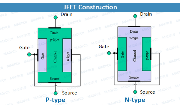
JFET Construction
Polarities
P-type and N-type polarities of Junction Field Effect Transistors are shown in following figure. In each case, the voltage between the gate and source is such that the gate is reverse biased. The source and the drain terminals are interchangeable.
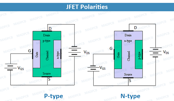
JFET Polarities
The following points may be noted:
- The input circuit (i.e. gate to source) of a junction FET is reverse biased. This means that the device has high input impedance.
- The drain is so biased w.r.t. source that drain current ID flows from the source to drain.
- In all junction FETs, source current (IS) equals to the drain current i.e IS = ID.
Principle
The two PN junctions at the sides form two depletion layers. The current conduction by charge carriers (i.e. electrons) is through the channel between the two depletion layers and out of the drain. The width and hence resistance of this channel can be controlled by changing the input voltage VGS. The greater the reverse voltage VGS, the wider will be the depletion layer and narrower will be the conducting channel. The narrower channel means greater resistance and hence source to drain current decreases. Reverse will happen when VGS decreases. Thus, JFET operates on the principle that width and hence resistance of the conducting channel can be varied by changing the reverse voltage VGS. In other word, the magnitude of drain current ID can be changed by altering VGS.
How Does It Work?
The working of junction FET can be explained as follows:
- Case I: When a voltage VDS is applied between drain and source terminals and voltage on the gate is zero, the two PN junctions at the sides of the bar establish depletion layers. The electrons will flow from source to drain through a channel between the depletion layers. The size of the depletion layers determines the width of the channel and hence current conduction through the bar.
- Case II: When a reverse voltage VGS is applied between gate and source terminals, the width of depletion layer is increased. This reduces the width of conducting channel, thereby increasing the resistance of n-type bar. Consequently, the current from source to drain is decreased. On the other hand, when the reverse bias on the gate is decreased, the width of the depletion layer also decreases. This increases the width of the conducting channel and hence source to drain current.
A p-channel JFET operates in the same manner as an n-channel JFET except that channel current carriers will be the holes instead of electrons and polarities of VGS and VDS are reversed.
Differences Between JFET and BJT
The JFET differs from an ordinary BJT in the following ways:
- In a junction FET, there is only one type of carrier, i.e. holes in p-type channel and electrons in n-type channel. For this reason it is also called unipolar transistor. However, in an ordinary BJT, both electrons and holes play role in conduction. Therefore, it is called as bipolar transistor.
- As the input circuit of a JFET is reverse biased, therefore, it has a high input impedance. However, the input circuit of a BJT is forward biased and hence has low input impedance.
- The primary functional difference between the JFET and BJT is that no current enters the gate of JFET. However, in typical BJT base current might be a few µA.
- A BJT uses the current into its base to control a large current between collector and emitter. Whereas a JFET uses voltage on the gate terminal to control the current between drain and source.
- In junction FET, there is no junction. Therefore, noise level in junction FET is very small.
Advantages of JFET
A JFET is a voltage controlled, constant current device in which variation in input voltage control the output current. Some of the advantages are:
- It has a very high input impedance. This permits high degree of isolation between the input and output circuits.
- The operation of a JFET depends upon the bulk material current carriers that do not cross junctions. Therefore, the inherent noise of tubes and those of transistors are not present in a JFET.
- A JFET has a negative temperature co-efficient of resistance. This avoids the risk of thermal runaway.
- A JFET has a very high-power gain. This eliminates the necessity of using driver stages.
- A JFET has a smaller size, longer life and high efficiency