Table of Contents
What’s A Via Hole in PCB?
Via (Vertical Interconnect Access) on printed circuit board (PCB) consists of two pads (annular rings) in corresponding position on different layers of the board, that are electrically connected by a hole through the board. The hole is made conductive by electroplating, or is lined with a tube or a rivet. (Source: Via (electronics) – Wikipedia)
A via consists of:
- Barrel – conductive tube filling the drilled hole
- Pad -connects each end of the barrel to the component, plane, or trace
- Antipad -clearance hole between barrel and metal layer to which it is not connected
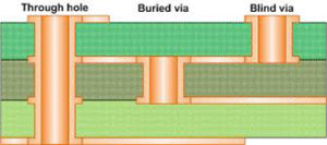
There are 3 basic kinds of vias:
- Plated Through Hole (PTH): drilled from the top and go completely through the bottom of the board
- Blind Via: exposed only on one side of the board
- Buried Via: connect internal layers without being exposed on either surface
Vias are used to electrically connection, and thermally join traces, pads, and polygons on different layers of a PCB. Except for PTH, Blind and buried vias, there is another kind, called Thermal Vias, which carry heat away from power devices and are typically used in arrays of about a dozen.
How to Make PCB Vias?
Briefly, holes are drilled through copper pads on the PCB, a chemical is put in the hole to dissolve epoxy on the internal layers to further expose the interior layer copper pads. Finally, a bit of copper is put in the hole with electroplating. With standard PCB manufacturing process, possible via configurations are limited to through-holes. Depth-controlled drilling techniques such as using lasers can allow for more varied via types.
Vias are with openings, which can collect tin solder in the process of reflow soldering of PCB assembly. For prevent short, a protective method can be applied – covering the vias openings with solder mask, which is called Vias Tenting. For more details of vias treatment, please click and refer to our Vias Protection.
Via Configurations
PCB manufacturing typically starts with a so-called core, a basic double-sided PCB. Layers beyond the first two are stacked from this basic building block. If two more layers are consecutive stacked from bottom core, you can have a 1-2 via, a 1-3 via and a through hole. Each type of via is made by drilling at each stacking stage. If one layer is stacked on top of the core and other is stacked from the bottom, the possible via configurations are 1-3, 2-3 and through hole. The user must gather information about the PCB manufacturer’s allowed methods of stacking and possible vias. For cheaper boards, only through holes are made and antipad (or clearance) is placed on layers which are supposed not to be connected to vias.
Using Cross-section to Examine Via Quality
How to inspect the via quality of a printed circuit board? As a manufacturer, MADPCB puts sacrificial vias on PCBs on a section of the production board. The vias are then sliced, and the cross-sections are examined to determine the effectiveness of the electroplating process. With a cross-section, we can visual check the via copper wall thickness and measure the dimple of blind microvias.
When to Use Vias?
Vias provide a path for electrical and thermal energy to move from layer to layer on PCB board. Generally, the more energy being dissipated by an IC, the more vias it should have connecting its thermal pad to the underlying copper layers that can be distribute the thermal energy.
For parts of your circuit carrying power, or fast signals, use multiple vias to connect layer to layer. It is generally better to have several smaller vias than one large via. The design choice reduces inductance and provides additional paths for current in case one of the vias fails.
For a simple double-sided board, your only option is a through via hole. For multilayer boards, you might also be able to specify blind or buried vias in your design at increased cost. It is often the case that a via needs to form an electrical connection between internal and external layers. The use of a through-hole via in such situations places an unused hole (and possibly an unused pad) onto other layers, and this consumes PCB real estate and interferes with routing on adjacent layers, but it is the cheapest and most reliable option. Blind vias can free up real estate by creating a connection between the two layers and a hole only on the layers in between. Buried vias are not often used due to expense, reliability concerns, and difficulty of troubleshooting.

