Table of Contents
Any Layer HDI PCB Microvia III-Any Layer Microvia
Any Layer HDI PCBs are those multilayer PCBs that enable free connection between all layers combing laser technology and filled plating technology that allows ultra-fine processing. So Any Layer HDI PCB Microvia III-Any Layer Microvia With the higher degree of design freedom and higher-density wiring, these PCBs are ideal for the needs of downsizing and thinning of smartphones and other high-performance electronic devices.
Features
- Any layer HDI PCBs with laser via and filled plating on each layer
- Thinner 0.4mm pitch CSP by any layer interconnection supported
- Mass-production of 10-layer μVia III (AnyLayer PCBs) for mobile devices
Applications
Industry demand for smaller products demands higher circuitry density in circuit boards. Any-Layer Vias span a wide range of industries such as Automotive, Industrial/Consumer and Telecom.
Cross-Section

Any Layer HDI PCB Microvia III Cross-Section
Stack-up
AnyLayer Interconnect PCB Microvia III Stackup
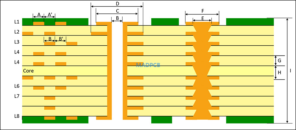
Design Rule
|
Parameter |
Symbol | Standard Spec
(μm) |
Min Spec
(μm) |
||
| Trace Width/Spacing | HDI Layer | A/A’ | 75/75 |
50/50 |
|
|
Plated Through Hole |
Pad Diameter | Outer Layer | B | 300 | 250 |
| Inner Layer | C | 550 |
450 |
||
|
Laser Via |
Via Diameter | E | 100 | 75 | |
| Pad Diameter | F | 250 |
220 |
||
|
Dielectric Thickness |
HDI Layer | G | 60 | 40 | |
| Core Layer | H | 60 |
50 |
||
|
PCB Thickness |
6-Layer | I | 440 | ||
|
8-Layer |
590 |
||||
| 10-Layer |
740 |
||||
Click to know our PCB Capabilities and Fabrication Process.