What Is a Coplanar in PCB?
PCB Coplanar waveguide is a type of electrical transmission line, which is routed in outer or inner layers of a printed circuit board (PCB) in the middle of two grounded traces with or without a ground plane layer. This technique is preferably used in a multilayer PCB design, and the signal trace is backed either with or without by the ground plane below. This transmission line is used to convey microwave-frequency signals.
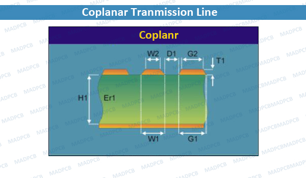
Coplanar Transmission Line
Among various RF waveguide structures used from high frequency layout and routing, coplanar waveguide design is probably the most common. There are some particular reasons for this, many of which stem from its ease of placement on the surface layer of PCB. Coplanar waveguide designs are easy to route in an RF PCB layout, and they are normally used for controlled impedance routing. This is quite important for RF applications, where a signal often needs to be routed to an amplifier, mixer, antenna, or other RF component.
Coplanar Waveguide Design
All coplanar waveguides come in two variants: standard coplanar waveguide and grounded coplanar waveguide. The standard coplanar waveguide can be placed above a ground plane, or it can be placed without ground. Both are designed for routing on the surface layer, although you can create variations that operate in an internal layer.
There are some advantages to using a coplanar waveguide design over a standard microstrip or stripline design:
- High isolation: This is probably the most common reason for using a coplanar waveguide design. Although the waveguide is routed on the surface layer, it will have some lateral isolation thanks to the surrounding ground planes. This is the same reason ground pour is used to fill in the surface layer routed with low-speed traces: it provides additional EMI shielding and terminates field lines emanating from the trace.
- Lower loss than striplines: A stripline and some other waveguides, such as substrate integrated waveguides, confine the field entirely to the substrate, so the wave sees entirely a lossy PCB substrate. In a coplanar waveguide, much of the field lines pass through the region above the dielectric, so they will not experience as much loss.
- Tunable bandwidth: The bandwidth of the structure can be tuned by adjusting the geometry. Coplanar waveguides used at ~5 GHz can be quite large, but the bandwidth can be confined to just the frequency range needed for single-mode propagation.
- Single mode propagation: The fact that the bandwidth is tunable means that we can limit the bandwidth to just the value needed for a single mode (normally TE-mode in fenced waveguides).
- Single mode propagation: The fact that the bandwidth is tunable means that we can limit the bandwidth to just the value needed for a single mode (normally TE-mode in fenced waveguides).
As part of coplanar waveguide design, there are two primary quantities that need to be calculated: impedance and effective dielectric constant (this has basically the same meaning as that for microstrip traces). The primary mathematical tool used for these calculations is the elliptical integral of the first kind, which arises due to the use of conformal mapping for deriving wave impedance in these structures.