What is P-N Junction?
P-N Junction or PN Junction is a boundary or interface between two types of semiconductor materials, p-type and n-type, inside a single crystal of semiconductor. The “p” (positive) side contains an excess of holes, while the “n” (negative) side contains an excess of electrons in the outer shells of the electrically neutral atoms there. This allows electrical current to pass through the junction only in one direction. The p-n junction is created by doping, for example by ion implantation, diffusion of dopants, or by epitaxy (growing a layer of crystal doped with one type of dopant on top of a layer of crystal doped with another type of dopant). If two separate pieces of material were used, this would introduce a grain boundary between the semiconductors that would severely inhibit its utility by scattering the electrons and holes.
p–n junctions are elementary “building blocks” of semiconductor electronic devices such as diodes, transistors, solar cells, LEDs, and integrated circuits; they are the active sites where the electronic action of the device takes place. For example, a common type of transistor, the bipolar junction transistor, consists of two p–n junctions in series, in the form n–p–n or p–n–p; while a diode can be made from a single p-n junction. A Schottky junction is a special case of a p–n junction, where metal serves the role of the n-type semiconductor.
Properties
The p–n junction possesses essential properties for modern electronics. A p-doped semiconductor is relatively conductive. The same is true of an n-doped semiconductor, but the junction between them can become depleted of charge carriers, and hence non-conductive, depending on the relative voltages of the two semiconductor regions. By manipulating this non-conductive layer, p–n junctions are commonly used as diodes: circuit elements that allow a flow of electricity in one direction but not in the other (opposite) direction. Bias is the application of a voltage across a p–n junction; forward bias is in the direction of easy current flow, and reverse bias is in the direction of little or no current flow.
The forward-bias and the reverse-bias properties of the p–n junction imply that it can be used as a diode. A p–n junction diode allows electric charges to flow in one direction, but not in the opposite direction; negative charges (electrons) can easily flow through the junction from n to p but not from p to n, and the reverse is true for holes. When the p–n junction is forward-biased, electric charge flows freely due to reduced resistance of the p–n junction. When the p–n junction is reverse-biased, however, the junction barrier (and therefore resistance) becomes greater and charge flow is minimal.
Equilibrium (zero bias)
In a p–n junction, without an external applied voltage, an equilibrium condition is reached in which a potential difference forms across the junction. This potential difference is called built-in potential Vbi.
At the junction, the free electrons in the n-type are attracted to the positive holes in the p-type. They diffuse into the p-type, combine with the holes, and cancel each other out. In a similar way the positive holes in the p-type are attracted to the free electrons in the n-type. The holes diffuse into the n-type, combine with the free electrons, and cancel each other out. The positively charged, donor, dopant atoms in the n-type are part of the crystal, and cannot move. Thus, in the n-type, a region near the junction becomes positively charged. The negatively charged, acceptor, dopant atoms in the p-type are part of the crystal, and cannot move. Thus, in the p-type, a region near the junction becomes negatively charged. The result is a region near the junction that acts to repel the mobile charges away from the junction through the electric field that these charged regions create. The regions near the p–n interface lose their neutrality and most of their mobile carriers, forming the space charge region or depletion layer.

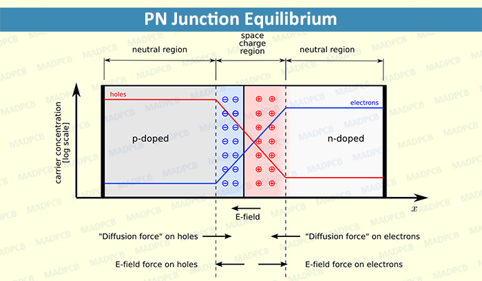
PN Junction Equilibrium
The electric field created b the space charge region opposes the diffusion process for both electrons and holes. There are two concurrent phenomena: the diffusion process that tends to generate more space charge, and the electric field generated by the space charge that tends to counteract the diffusion. The carrier concentration profile at equilibrium is shown in figure A with blue and red lines. Also shown are the two counterbalancing phenomena that establish equilibrium.
The space charge region is a zone with a net charge provided by the fixed ions (donors or acceptors) that have been left uncovered by majority carrier diffusion. When equilibrium is reached, the charge density is approximated by the displayed step function. In fact, since the y-axis of figure A is log-scale, the region is almost completely depleted of majority carriers (leaving a charge density equal to the net doping level), and the edge between the space charge region and the neutral region is quite sharp. The space charge region has the same magnitude of charge on both sides of the p–n interfaces, thus it extends farther on the less doped side in this example.
Also see
