What Is Plastic Leaded Chip Carrier?
Plastic Leaded Chip Carrier (PLCC) is a four-sided “J” leaded plastic body package. PLCC is a form of SMD integrated circuit (IC) package that can be used to be enable ICs to be mounted on a printed circuit board (PCB) either directly soldered to the board or within a socket. The PLCC “J” Lead configuration requires less board space versus equivalent gull leaded components.
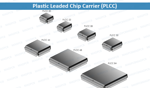
Plastic Leaded Chip Carrier (PLCC)
*Notes
- All PLCCs have “J” leads
- Standard lead pitch is 1.27mm (50 mils)
- PLCCs are to JEDEC standards
- Tube quantity may vary
- 13″ reels are standard
- Parts available on Tape and Reel
- Moisture sensitivity is JEDEC level 3
- Lead-free parts are available with 100% Matte Sn finish
SMD PLCC Basics
An SMD PLCC or plastic leaded chip carrier is a four-sided flat IC package or chip carrier. Rather than using the gull wing leads that are used on the quad flat pack, the SMD PLCC uses a “J” lead format. Here the leads are in the form of a J that is positioned on the edge of the SMD PLCC package with the lower section of the J folding back under the package.
As a result of the lead format the SMD PLCC offers a number of advantages:
- Socket compatible: In some areas, especially when developing new products a socketed chip can be particularly useful, if new builds of a PLD or other chip may be needed. The PLD can be programmed off the board and added to the board to test the overall system operation. While many boards will allow on-board programming, this may not always be achievable.
- Space saving: The “J” lead of the SMD PLCC provides a useful reduction in board area when compared to the gull wing lead of the QFP. As the “J” lead effectively folds back under the package, this provides a significant reduction in real estate usage.
- Heat resistance: In some limited instances, the heat experienced during the soldering process could cause damage to the chip. In this case a socket can be added to the board, and the PLCC inserted after soldering is completed, and no high temperatures will be experienced.
The SMD PLCC can have a variety of formats. PLCC packages are available in a variety of lead counts, from 20 to 84, and are also common for 2-pin LED components. The main advantage of PLCC packages, both in terms of design and PCB production, comes into play for prototype designs where extensive IC Programming is required.
PLCC Sockets
One of the major advantages of an SMD PLCC is that the chip can be connected to the circuit via a socket. The same chip format can also be used in the standard SMT format, soldering the PLCC directly to the board. This can have significant advantages when a replaceable chip is needed for development, but then the same chip can be used in production where it can be soldered onto the board.
PLCC sockets may either be surface mounted – the most common, or some through hole versions are also available. Some through hole PLCC sockets may be used with wire wrap techniques for prototyping.
Although it is often possible to extract PLCCs using a small screwdriver, etc., it is far more preferable to use a PLCC extractor tool. This will make extraction of the PLCC far easier, and minimize the possibility of any damage.
The PLCC package fills a gap in the marketplace. Although not as widely used as other forms of IC package, it can be useful in applications where a the design may not be completely stable and firmware updates may be required and the design is such that this may not be possible in situ.