What Is Resonance in PCB?
PCB Resonance exists when the inductive reactance (XL) and the capacitive reactance (XC) are of equal magnitude, causing electrical energy to oscillate between the magnetic field of the inductor and the electric field of the capacitor. In some circuits, this happens when the impedance between the input and output of the circuit is almost zero and the transfer function is close to one. Resonant circuits exhibit ringing and can generate higher voltages or currents than are fed into them. They are widely used in wireless (radio) transmission for both transmission and reception.
Resonance occurs because the collapsing magnetic field of the inductor generates an electric current in its windings that charges the capacitor and the discharging capacitor provides an electric current that builds the magnetic field in the inductor, and the process is repeated.
At resonance, the series impedance of the two elements is at a minimum and the parallel impedance is a maximum. Resonance is used for tuning and filtering, because resonance occurs at a particular frequency for given values of distortion and damage to circuit elements.
At resonance the inductive reactance and the capacitive reactance are of equal magnitude. Therefore, ωL = 1/ωC, where ω=2πf, in which f is the resonant frequency in hertz (Hz), L is the inductance in henrys (H), and C is the capacity in farads (F) when standard SI units are used. Thus, f=π/(2√LC)
How to Think about Your Electronics?
PCB designers often think about electronics in terms of circuit diagrams and equivalent circuits, but this eventually breaks down and we have to consider the high frequency characteristics of real electronic systems. In real printed circuit boards (PCBs), the propagating characteristics of electrical signals will dominate system behavior, including for something as simple as DC power distribution. DC power, particularly as it is drawn into a board by integrated circuits, is not really DC, which creates strongly resonant excitation in a PCB.
The power and ground plane arrangement in your PCB form the basis of power distribution throughout your board and need to provide stable power to components. In reality, there are important transient effects that occur in any circuit board and the structure of plane layers in the board plays a role in determining the emission spectrum at very high frequencies. This is where power plane resonance analysis becomes useful for understanding where the circuit description of a PDN (Power Delivery Network) ends and where you’ll need to think about your plane arrangement in terms of waveguide behavior.
Power Plane Resonance Analysis
If you’ve ever looked at an impedance plot for the PDN in your PCB, you’ll notice that the plot has some resonant behavior at high frequencies. These frequencies generally fall into the GHz range and higher, depending on the structure and size of your circuit board. When the power and ground planes overlap in a PCB, the structure they create will form a semi-parallel waveguide that has some distinct resonance. The image below shows an example PDN impedance spectrum measured on a PCB, which includes resonances that can be seen at high frequencies.
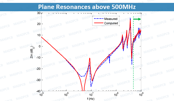
Plane Resonances above 500MHz
All real power plane arrangements in a PCB have some resonances, and these resonances can be excited by emission of a propagating electromagnetic wave in the structure. All resonances in a PDN can be calculated by considering the structure of the system, which looks a lot like a parallel plate waveguide. While we might like to think the PDN acts exactly like a parallel plate waveguide, this is only an approximation; all other conductors that traverse the region like a parallel plate waveguide, this is only an approximation; all other conductors that traverse the region between the planes in a PCB will modify the resonant frequencies from the values calculated for a parallel plate waveguide. In addition, the finite span of the PDN will determine the resonances in the structure, leading to a modification of the parallel plate waveguide resonances into cavity resonances.
For a board with dimensions a and b, and with spacing between power and ground given by h, the resonant frequencies are:

Although the formula above is not universally applicable to every PDN structure, it gives us a good approximation for the lowest order PDN resonance. Typical values for the lowest order PDN impedance range from 100MHz to above 1GHz, depending on the dimensions of the board and the spacing between planes in the structures.
The chip also has its own PDN, so logic would dictate that it also exhibits some resonances that can be excited by an incoming transient oscillation on the board’s power rails. However, this is not the case except up to extremely high frequencies simply due to the geometry of the chip and its PDN.
The Transition from Board to Chip
Once the incident wave from the power supply impinges on the chip, the voltage measured on the chip’s power rails will be very different from that measured on the board’s power rails. An integrated circuit has much smaller separation between the power rails and the ground plane to the die, so the power plane resonances will be located at much higher frequencies.
The image below shows an example simulation of the PDN impedance measured in three different ways. The blue curve shows a typical PDN impedance curve for a CMOS integrated circuit measured on the main power rail for the chip. This is the type of curve that would be measured directly on the die after any passive regulation section; note that this does not include pin-package inductance due to the bond wire or lead frame. This is placed in parallel with the board impedance, which is assumed to be strongly decoupled and has relatively flat impedance above 10kHz. The red curve shows the parallel equivalent of these two impedances.
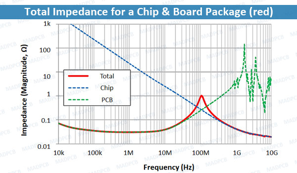
Total Impedance for a Chip & Board Package (red)
In this example, the total impedance shows an antiresonance at ~100MHz, but it is relatively weak with only ~1Ohm impedance. The rest of the curve is quite flat and overlaps with the low impedance portion of the board at low frequencies, and with the chip’s PDN impedance at high frequencies. The chip PDN also has high impedance resonance/anti-resonance pairs, but they are at such high frequencies that they cannot be seen in the above window. The presence of chip caps on the PDN also helps keep the total impedance low as measured on the chip.
Just as an example, we can compare the impedances of the lowest order waveguide modes for the board and chip in a simple exercise. In the above example, the lowest order board resonance is only 2GHz; if we assume the power rail to ground distance on the die is only a factor 10 smaller than on the PCB with ~1cm² chip dimensions, then the lowest order resonance in the chip PDN is will already exceed 20GHz. The exact resonant frequencies in a complex structure like the PDN on an integrated circuit (IC) or a circuit board shouldn’t be treated with circuit models. Instead, these resonances are best determined with a field solver application that pulls data directly from the physical PCB layout.
The best way to suppress analog signal resonance is to ensure impedance matching throughout your board. This is best done when you use impedance-controlled design in your PCBs. This ensures that your traces will have consistent impedance throughout your board (50 Ohms, or 100 Ohms for differential pairs), and you will only need to worry about impedance matching components to your trace impedance.
Impedance controlled PCB design requires selecting the appropriate trace geometry and arrangement to use throughout the board in order to guarantee impedance matching within the limits defined by manufacturing tolerances. A designer with the right software can specify matching constraints that ensure signal resonance does not cause major problems in your analog or mixed signal board.