What is a Full Wave Rectifier?
A Full Wave Rectifier is defined as a type of rectifier that converts both halves of each cycle of an alternating wave (AC signal) into a pulsating DC signal. Full-wave rectifiers are used to convert AC voltage to DC voltage, requiring multiple diodes to construct. Full wave rectification is the process of converting an AC signal to a DC signal.
Circuits that convert AC current into DC are known as rectifiers. If such rectifiers rectify both the positive and negative half cycles of an input alternating waveform, the rectifiers are full-wave rectifiers.
Full-wave rectifiers achieve this by using a group of diodes. A diode permits current in one direction only and blocks the current in the other direction. We use this principle to construct various rectifiers.
We can classify rectifiers into two types:
- Half Wave Rectifier
- Full Wave Rectifier
When we use a half-wave rectifier, a significant amount of power gets wasted as only one half of each cycle passes through, and the other cycle gets blocked. Moreover, the half-wave rectifier is not efficient (40.6%), and we can not use it for applications that need a smooth and steady DC output. For a more efficient and steady DC output, a full wave rectifier is used.
We can further classify them into:
- Center-tapped Full Wave Rectifier
- Full Wave Bridge Rectifier
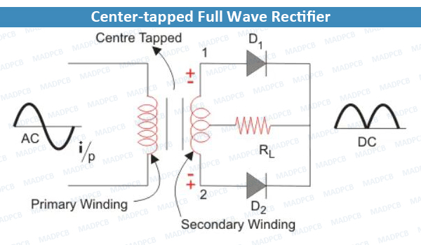
Center-tapped Full Wave Rectifier
Full Wave Bridge Rectifier
Center-tapped Full Wave Rectifier
A center-tapped full-wave rectifier system consists of:
- Center-tapped Transformer
- Two Diodes
- Resistive Load
Center-tapped Transformer: – It is a normal transformer with one slight modification. It has an additional wire connected to the exact center of the secondary winding.
This type of construction divides the AC voltage into two equal and opposite voltages, namely +Ve voltage (Va) and -Ve voltage (Vb). The total output voltage is
V = Va + Vb
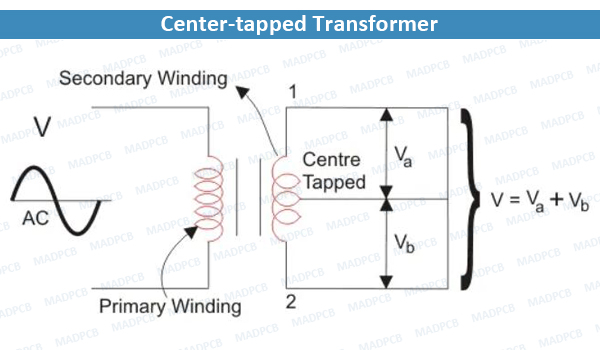
Center-tapped Transformer
The circuit diagram is as follows.
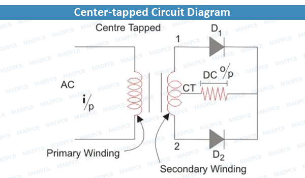
Center-tapped Circuit Diagram
Working of Center-tapped Full Wave Rectifier
We apply an AC voltage to the input transformer. During the positive half-cycle of the AC voltage, terminal 1 will be positive, center-tap will be at zero potential, and terminal 2 will be negative potential.
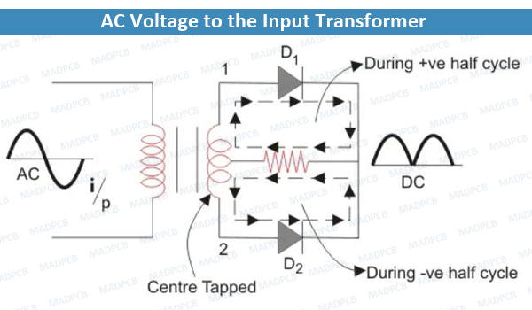
AC Voltage to the Input Transformer
This will lead to forwarding bias in diode D1 and cause current to flow through it. During this time, diode D2 is in reverse bias and will block current through it.
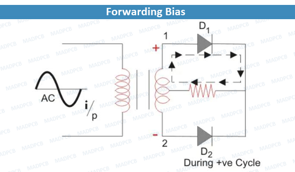
Forwarding Bias
During the negative half-cycle of the input AC voltage, terminal 2 will become positive relative to terminal 2 and center-tap. This will lead to forwarding bias in diode D2 and cause current to flow through it. During this time, diode D1 is in reverse bias and will block current through it.
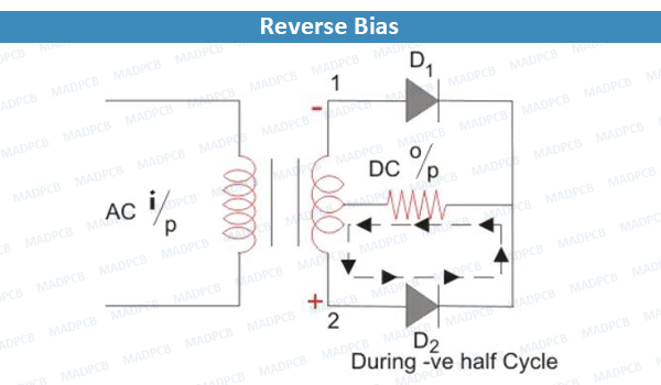
Reverse Bias
During the positive cycle, diode D1 conducts, and during the negative cycle, diode D2 conducts and during the positive cycle.
As a result, both half-cycles are allowed to pass through. The average output DC voltage here is almost twice the DC output voltage of a half-wave rectifier.
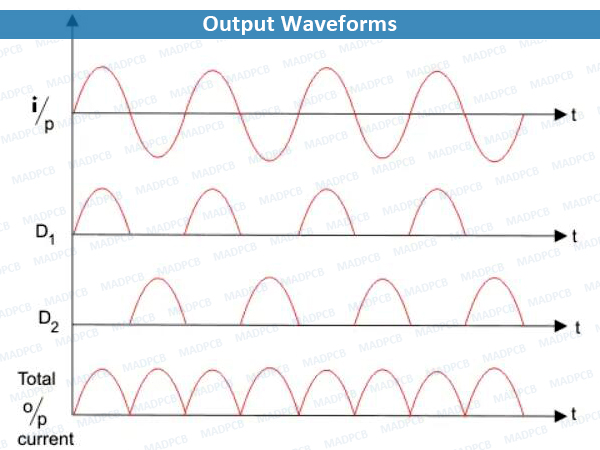
Output Waveforms
Filter Circuit
We get a pulsating DC voltage with many ripples as the output of the center-tapped one. We cannot use this pulsating for practical applications.
So, to convert the pulsating DC voltage to pure DC voltage, we use a filter circuit as shown above. Here we place a capacitor across the load.
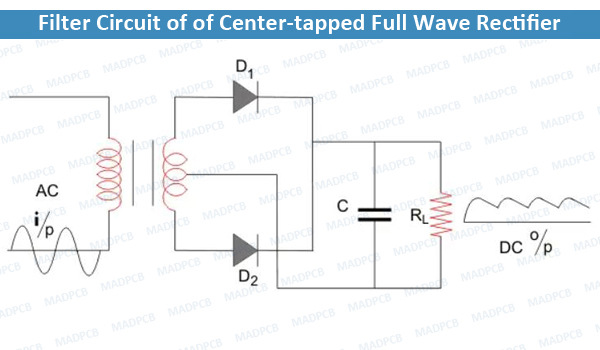
Filter Circuit of of Center-tapped Full Wave Rectifier
The working of the capacitive filter circuit is to short the ripples and block the DC component so that it flows through another path and is available across the load.
During the positive half-wave, the diode D1 starts conducting. The capacitor is uncharged.
When we apply an input AC voltage that happens to be more than the capacitor voltage, it charges the capacitor immediately to the maximum value of the input voltage. At this point, the supply voltage is equal to capacitor voltage.
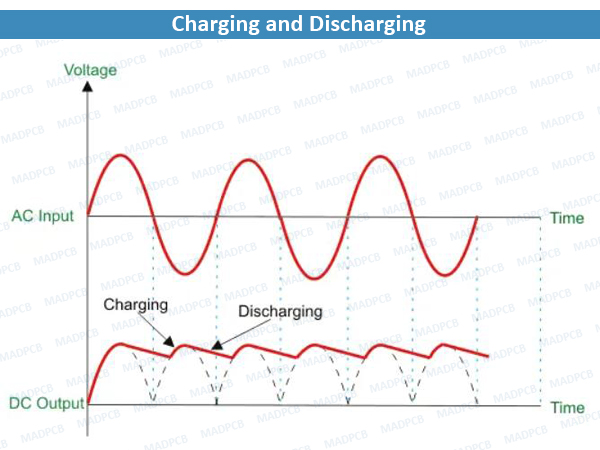
Charging and Discharging
When the applied AC voltage starts decreasing and less than the capacitor, the capacitor starts discharging slowly, but this is slower when compared to the charging of the capacitor, and it does not get enough time to discharge entirely, and the charging starts again.
So around half of the charge present in the capacitor gets discharged. During the negative cycle, the diode D2 starts conducting, and the above process happens again.
This will cause the current to flow in the same direction across the load.
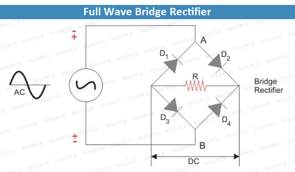
Full Wave Bridge Rectifier
A full wave bridge rectifier is a rectifier that will use four diodes or more than that in a bridge formation. A full wave bridge rectifier system consists of
- Four Diodes
- Resistive Load
We use the diodes, namely A, B, C and D, which form a bridge circuit. The circuit diagram is as follows.
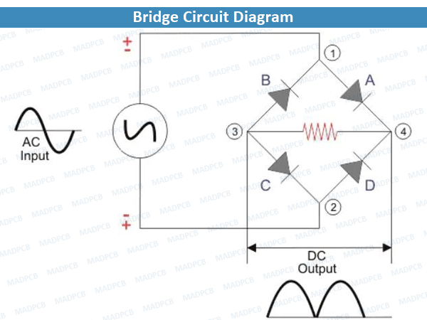
Bridge Circuit Diagram
Principle of Full Wave Bridge Rectifier
We apply an AC across the bridge. During the positive half-cycle, terminal 1 becomes positive, and terminal 2 becomes negative.
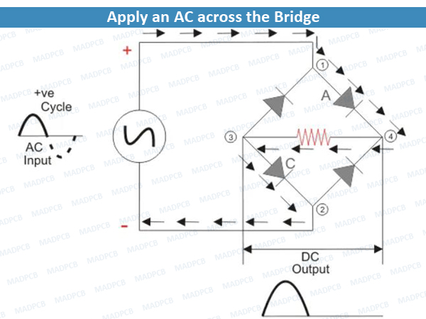
Apply an AC across the Bridge
This will cause the diodes A and C to become forward-biased, and the current will flow through it. Meanwhile, diodes B and D will become reverse-biased and block current through them. The current will flow from 1 to 4 to 3 to 2.
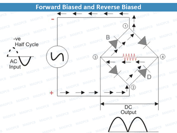
Forward Biased and Reverse Biased
During the negative half-cycle, terminal 1 will become negative, and terminal 2 will become positive.
This will cause the diodes B and D to become forward-biased and will allow current through them. At the same time, diodes A and C will be reverse-biased and will block the current through them. The current will flow from 2 to 4 to 3 to 1.
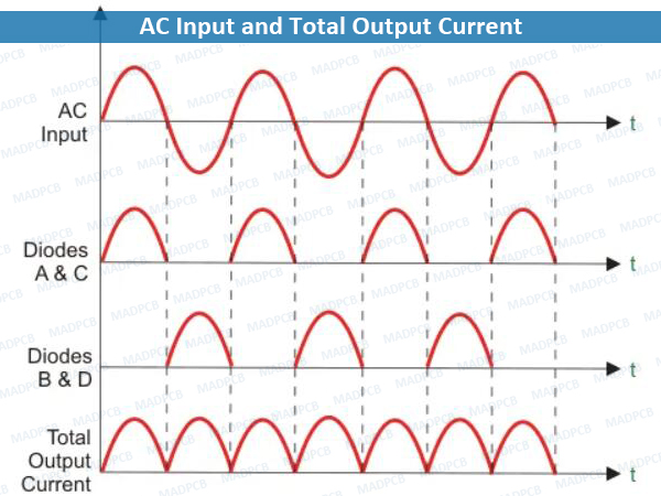
AC Input and Total Output Current
Filter Circuit of Full Wave Bridge Rectifier
We get a pulsating DC voltage with many ripples as the output of the full wave bridge rectifier. We can not use this voltage for practical applications.
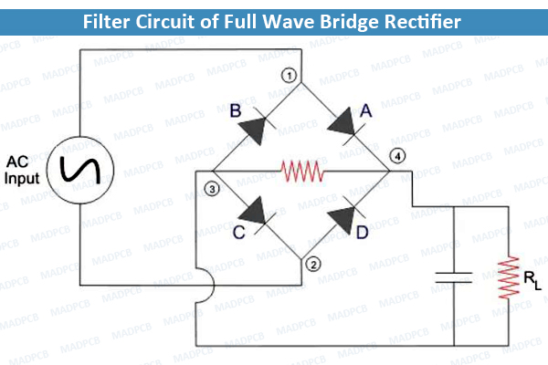
Filter Circuit of Full Wave Bridge Rectifier
So, to convert the pulsating DC voltage to pure DC voltage, we use a filter circuit as shown above. Here we place a capacitor across the load. The working of the capacitive filter circuit is to short the ripples and block the DC component so that it flows through another path, and that is through the load.
During the half-wave, the diodes A and C conduct. It charges the capacitor immediately to the maximum value of the input voltage. When the rectified pulsating voltage starts decreasing and less than the capacitor voltage, the capacitor starts discharging and supplies current to the load.
This discharging is slower when compared to the charging of the capacitor, and it does not get enough time to discharge entirely, and the charging starts again in the next pulse of the rectified voltage waveform.
So around half of the charge present in the capacitor gets discharged. During the negative cycle, the diodes B and D start conducting, and the above process happens again. This causes the current to continue to flow through the same direction across the load.
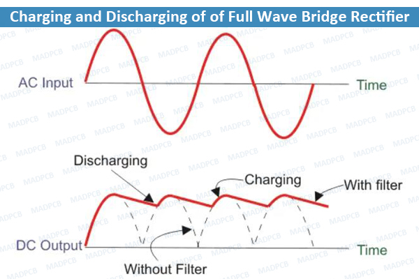
Charging and Discharging of of Full Wave Bridge Rectifier
Full Wave Rectifier Formula
We will now derive the various formulas for a full wave rectifier based on the preceding theory and graphs above.
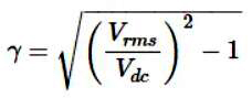
Ripple Factor (γ)
‘Ripple’ is the unwanted AC component remaining when converting the AC voltage waveform into a DC waveform.
Even though we try out best to remove all AC components, there is still some small amount left on the output side which pulsates the DC waveform. This undesirable AC component is called ‘ripple’.
To quantify how well the half-wave rectifier can convert the AC voltage into DC voltage, we use what is known as the ripple factor (represented by γ or r).
The ripple factor is the ratio between the RMS value of the AC voltage (on the input side) and the DC voltage (on the output side) of the rectifier.
The formula for ripple factor is:
Ripple Factor
Where Vrms is the RMS value of the AC component, and Vdc is the DC component in the rectifier.
The ripple factor of a center-tapped full-wave rectifier is equal to 0.48 (i.e. γ = 0.48).
Note: To construct a good rectifier, we need to keep the ripple factor as minimum as possible. We can use capacitors or inductors to reduce the ripples in the circuit.
Efficiency (η)
Rectifier efficiency (η) is the ratio between the output DC power and the input AC power. The formula for the efficiency is equal to:
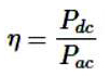
Rectifier efficiency (η)
The efficiency of a center-tapped full-wave rectifier is equal to 81.2% (i.e. ηmax = 81.2%).
Form Factor (F.F)
The form factor is the ratio between RMS value and average value.
The formula for form factor is given below:
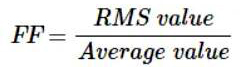
Form Factor
The form factor of a center-tapped full wave rectifier is equal to 1.11 (i.e. FF = 1.11).
Advantages of Full Wave Rectifiers
- Full wave rectifiers have higher rectifying efficiency than half-wave rectifiers. This means that they convert AC to DC more efficiently.
- They have low power loss because no voltage signal is wasted in the rectification process.
- The output voltage of a center-tapped full wave rectifier has lower ripples than a halfwave rectifiers.
Disadvantages of Full Wave Rectifiers
- The center-tapped rectifier is more expensive than a half-wave rectifier and tends to occupy a lot of space.