Power Supply in PCB
Power is the amount of energy transferred or converted per unit time. The SI unit is watt (W), equal to one joule (J) per second (s). The dimension of it is energy divided by time. It is the rate with respect to time at which work is done; it is the time derivative of work.
Whether your next PCB assembly runs on battery, a solar element, or plugs into the wall, you’ll need to design circuitry to regulate the power leading to your device. PCB power supply design can encompass more than just an actual power supply; systems ranging from PCs to home appliances need a power supply to convert AC power from the wall to DC power with low noise content.
The design is about more than just converting between AC and DC. There are power and signal integrity issues to consider, as well as thermal management issues. In fact, signal and power integrity are intimately related due to the way ICs operate, and some power supplies can produce significant radiated EMI that affects other parts of a printed circuit board PCB).
No power supply or the system connected to it is immune from signal integrity or power integrity problems, but implementing some simple design procedures can help prevent a redesign. These best practices include everything from proper component arrangement to decoupling/bypassing, and stackup design.
Design Options
The first step is to choose the type of power supply you wish to use for your device. Unregulated power supplies are a down-and-dirty option for converting AC power from a wall outlet to a DC voltage. The output from these supplies will contain a ripple waveform as the output is not smoothed with a regulator. Modern applications use a regulated power supply, where this ripple is minimized.
There are two principal options for regulating DC output from power supplies: using a linear regulator or a switching regulator, which is sometimes called a switch-mode power supply. These types pass the DC output from a full wave rectifier to a regulation circuit, which smooths the ripple waveform that is superimposed on the desired DC output. These regulators can also be used to directly regulate a DC power source like a battery. Linear regulators have very low noise, but they tend to be bulky due to the use of heatsinks or other active cooling measures required for thermal management. The significant heat dissipation in these power supplies is responsible for their low efficiency.
In contrast, a switched mode provides much higher efficiency over a broad current range, allowing these to take on smaller form factor. However, these use a PWM circuit to smooth and regulate the output voltage, which requires the use of an active switching component (normally a MOSFET). This means that the system radiates strong EMI, and the output will contain spikes due to switching noise. This switching noise can appear as a ringing signal on the output (i.e., conducted EMI), and this noise needs to be filtered from the output.
Design Practices
For low power applications, linear regulators and switching regulators are available as integrated circuits. These ICs are ideal for mobile devices or other devices that might plug into a wall outlet but require low power consumption. There are some basic PCB design considerations to take into account in order to ensure power integrity and signal integrity.
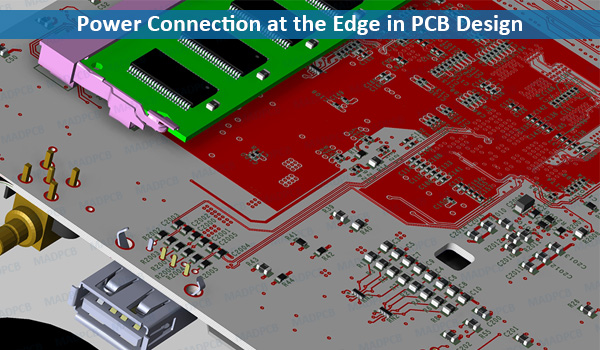
Power Connection at the Edge in PCB Design
Depending on the type of regulator used, there are some circuits you should consider adding to your board, and there are some simple PCB layout choices that can help suppress conducted and radiated EMI. In the extreme case, such as with a high current power supply or generally with a switching regulator, you may need to include shielding in your board to ensure signal integrity in nearby circuits.
- Thermal and Power Integrity: PCB power supply design is about more than just power conversion. Ensuring power integrity in the output from your power supply will help solve some signal integrity issues. Thermal management is also important as components will dissipate heat during the conversion process. Consider the following points during PCB power supply design.
- Choosing a Regulator: The output from linear and switching regulators includes some noise, although the source and effects of noise on your downstream circuits will vary. A linear regulator has less noise, but it is also less efficient and dissipates more heat. In contrast, a switching regulator replaces ripple on the input for switching noise on the output. However, it is easy to control the output voltage from a switching regulator (i.e., as a buck-boost converter) by adjusting the duty cycle of the PWM signal, which provides switching action. The switching regulator will dissipate much less heat thanks to its very high efficiency.
- Thermal Management Options: With high current power supplies, you’ll most likely be building a regulator circuit you need from discrete components as the size of the system will be too large to fit in a standard integrated circuit package. In this case, you will need to consider some thermal management options for any ICs in your power supply’s PCB. If you are converting power from a wall outlet to DC, one simple solution is to mount a fan on the enclosure and power it using the input AC signal. With DC-to-DC power supplies, you’ll need to use a PWM signal to run a fan to cool your components.
Your layer stack also plays a role in thermal management. Designing your power supply PCB on a multilayer board can aid thermal management as the internal copper plane layers help evenly distribute heat throughout the board. Using thermal vias and lands below components that dissipate a significant amount of heat can help quickly transport heat away from these components. The goal is to prevent hot spots from forming in your board by allowing heat to quickly dissipate from critical components.
Bypassing and Decoupling for Power Integrity
Once power is sent downstream to your components, various active components can cause ground bounce and ringing in a power bus when ICs switch. This can lead to bit rate errors when a large number of ICs switch simultaneously as it affects the power received by components and the potential difference between the ON and OFF states in digital signals. ICs that run at lower supply voltage are more prone to these problems as they have a smaller voltage difference between the ON and OFF states.
These problems can be solved by designing a decoupling network and by choosing bypass capacitors between the ground and power pins on an IC. The goal in placing bypass capacitors is to compensate changes in the ground potential when many ICs switch simultaneously. Similarly, a decoupling network is designed to transient oscillations (i.e., ringing) in the power bus when ICs on the bus switch. One tool for designing your power delivery network and decoupling network is to use circuit analysis tools to design the equivalent RLC network that forms these circuits. With the right component choices, you can critically damp transient oscillations in your power delivery network and compensate ground bounce.
Conducted EMI Suppression
Noise output from a regulator or from an unregulated power supply can impact downstream components and conducted EMI. Severe noise on the power bus can affect the output level from downstream components. Large ripple voltages and switching noise in a switching regulator can create these problems, especially when the power supply provides high current.
In this case, conducted EMI should be filtered from the power supply output. Since one generally desires a DC output, filtration can be used to remove these higher frequency components from the power supply output. This is where simulations for filters become important as this helps you choose the components you need to build your filter.
Shielding with Switching Regulators
Switching regulators emit EMI that can affect signal integrity in downstream circuits, especially in analog components. Low level switching regulators may not produce many problems unless they are placed very close to sensitive components. However, power supplies with high output current can cause involuntary switching in nearby digital circuits or noise spikes in analog circuits, which appear as a transient response in the nearby circuit.
Band stop filtering at the circuit’s natural frequency can be effective at removing these current spikes, but this is not practical when you are working with a large number of components on a board. Instead, it is easier to take advantage of shielding provided by ground planes in your layer stack and arrange sensitive components farther away from the switching regulator. You may need to place some shielding on sensitive components if they are near the switching regulator as this will block radiated EMI.